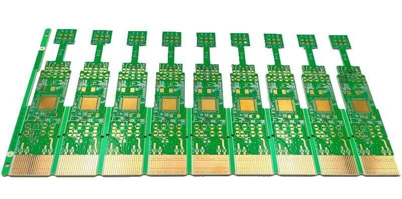
Ordinary gold finger, subsection gold finger, different length gold finger.
High-Quality Gold Finger PCBs with Competitive Pricing
- Normal, Subsection & Different Length Gold Finger
- Gold Plating up to 5µm
- Immersion Gold, Soft Gold & Hard Gold
- Single-layer, Double-layer & Multilayer
- ISO9001:2015 Certified & UL Listed
- 100% E-testing, AOI Inspection & Visual Inspection
Get a free quote now!
What is a Gold Finger PCB?
Get a free quote now!
Gold Finger PCBs are crucial for facilitating communication between circuit boards through their communication interfaces. The gold finger technology is used to process the edge communication interface of the circuit board. These PCBs feature gold-plated connectors, often referred to as “gold fingers,” which are located on one or more sides of the PCB. The copper pads on the top or bottom of the PCB are free from solder masks and are plated with a hard gold layer ranging from 10 to 100 micro-inches in thickness. The pads are uniform in size and alignment, resembling fingers, hence the name.
Gold finger PCBs are primarily used in devices that require frequent plugging and unplugging, such as USB flash drives and DDR4 RAM. Due to gold’s high conductivity and resistance to oxidation, these PCBs are the ideal choice in the electronics industry for such applications. However, due to the need for a thicker gold layer, gold finger PCBs tend to be more expensive than standard PCBs with immersion gold (ENIG).
Why Choose ESPCBA for Your Gold Finger PCB?
Experienced Team:
Over 16 years of experience in gold finger PCB manufacturing with skilled technicians and excellent customer service.
Excellent Quality Control:
Adhering to ISO9001 standards throughout the production process, ensuring high-quality gold finger PCBs.
Competitive Pricing:
We offer high-quality gold finger PCBs at competitive prices due to our efficient supply chain and skilled workforce.
Trusted by 1000+ Customers:
ESPCBA is a trusted provider of high-quality gold finger PCBs, with a global customer base.
Classification and Features of PCB Gold Fingers
Gold fingers are classified based on their design and placement. The common types include:
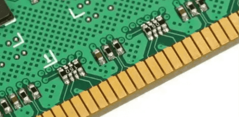
Ordinary Gold Finger:
Rectangular pads of uniform length and width placed neatly on the PCB edge.
Subsection Gold Finger:
Rectangular pads placed at varying positions on the PCB edge, with some pads disconnected.

Different Length Gold Finger:
Rectangular pads with varying lengths, located on the PCB edge.
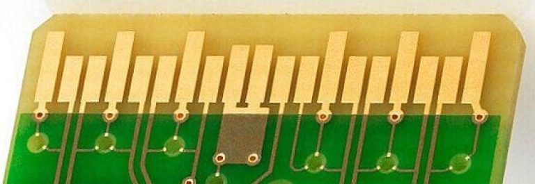
Gold fingers of different lengths are essential for ensuring proper fit in slots, reducing resistance, and maintaining electrical connection between PCBs and other device components. They also enhance durability due to gold’s corrosion resistance.
Two Main Technologies Used for Gold Finger Plating
Lead Wire Plating Method:
Gold is plated using lead wires from the gold finger edge. After plating, the wire is removed via milling or etching, but this method may leave lead wire residue.
No Lead Wire Method:
This technique avoids lead wire residues but may struggle with high-density circuit layouts, limiting its use in some situations.
Advantages and Disadvantages of Gold Finger Plating
Advantages
Gold plating provides a thickness of 3-50µm, offering high hardness, wear resistance, and oxidation resistance.
Disadvantages
The process is more costly, may result in short circuits, and has reduced solder strength. The skin effect may also impact high-frequency signal transmission.
Common Problems and Solutions in Gold Finger Plating
Cause: The concentration of gold needs to be increased; Proportion needs to be higher; Insufficient stir; nickel copper pollutes gold plating liquids.
Solutions: Add gold salt; Increase the proportion; Strengthen the stir; Clean the metal pollution.
Cause: Poor adhesion between copper and nickel; Poor adhesion between nickel and gold; Poor cleaning treatment before nickel and gold plating; High stress of nickel plating layer.
Solutions: Pay attention to the effect of copper treatment before nickel plating; Pay attention to the impact of nickel treatment before gold plating; Strengthen the treatment effect before plating; Purify plating liquid. Carry out towing or carbon treatment for nickel cylinders.
Cause: Too few additives; High PH value; Plating liquid was polluted by metal ions.
Solutions: Replenish moderate additives; Adjust the PH value; Remove the metal ions pollution. Pay attention to prevent pollution at ordinary times, especially the frequent Nickle ions pollution.
Cause: Clean and dry, not thorough; plating card edge connector PCB stock in a corrosive environment.
Solutions: Enhance cleaning and drying effect after gold plating; Plating gold PCB should stock far away from the corrosive environment.
Cause: The gold finger is exposed and touched with the air for a long time, and the surface of the gold finger will form an oxidation layer. Also, there will have dust adhesion causing the resistivity of the contact surface is increased, resulting in poor contact.
Solutions:
1. Using an ordinary eraser on the market can remove the oxidation layer and dust.
2. Use a pencil to remove the oxidation layer. The ingredients of the pencil are graphite and clay, clay has a certain hardness that can remove the oxide layer, and graphite are electric conductor, so if there is graphite residue after wiping the gold finger, it may cause a short circuit of adjacent contacts, therefor, after wiping the gold finger, should check if there is any graphite residue in the crevice. If there is, please be sure to clean it up.
3. Use PCB washing water. Use the cotton swab, cotton ball or dust-free cloth to dip in the washing water to wipe the golden finger. After drying completely, you can use it. If you can’t get any PCB washing water, you also can use the organic solvent of Anhydrous ethanol or Anhydrous isopropyl alcohol to replace it. Please avoid inhaling too much steam during operation to prevent health hazards from the gold finger PCBs.
Appearance Inspection Standards for Gold Finger PCB
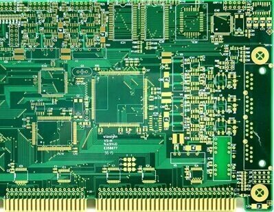
Gold fingers require a “solder mask opening” to ensure durability and avoid solder mask peeling, which could impact quality. Proper inspection standards are followed to check for convex angles, breaks, and scratches, ensuring the highest quality product.
Convex Angle
A. When the gap between two PCB gold fingers is greater than 0.38 mm ( 15mil ), it can accept a convex angle, but the space at least has two-thirds of the gap. B. When the gap between two PCB gold fingers is less than 0.38 mm ( 15mil ), this board can’t accept the convex angle phenomenon.
Break
The break area in a single PCB gold hand area shall not exceed 20%. If the break area is less than 20%, each side of the gold finger in PCB can’t be over two positions break ( including two positions).
Scratch
A. The scratch part of the PCB gold finger can not expose base material (copper or nickel). B. The scratch of a PCB gold finger without exposed substrate shall not exceed 1/5 of the PCB gold finger index on one side.
A Few Design Rules and Notes for PCB Gold Finger
- Ensure that the PCB gold finger is designed to meet industry requirements.
- Consider using a smaller plating thickness on the gold finger PCBs.
- Plating area is not allowed to place plating through holes.
- Do not add a solder mask or silkscreen on the plating area in the gold finger PCB.
- Gold finger position needs to make the whole solder mask opening treatment, and PIN does not need to make a stencil.
- Plan for any potential soldering operations.
- Keep an eye on overall cost efficiency.
- Pay attention to other components that may impact the PCB gold fingers' design.
- Use appropriate materials and surface finishes for the gold finger PCBs.
The Panel Mode for Gold Finger PCB
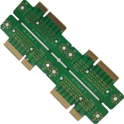
Without Side Strips:
Some manufacturers may struggle to add side strips, but ESPCBA can provide this service efficiently.
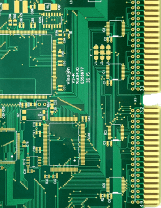
With Side Strips:
Standard panel mode places PCBs back to back, with gold fingers facing outward for easier production.
Function of Gold Finger Lead Wires
- Gold finger lead wires are used to interconnect PCBs and other electronic components. They provide electrical connections between the board and its external environment.
- The gold fingers serve as connectors for various devices, from computers, cell phones, DVD players, printers, home appliances etc. The gold-plated contacts also reduce corrosion caused by oxidation. Gold finger lead wires offer improved signal integrity for high-speed data transmissions.
- The gold finger lead wire is, therefore, an essential component for any device that requires connection to a PCB. It also provides reliability, durability and cost-effectiveness for any OEM application.
How to Remove the Gold Finger Lead Wire?
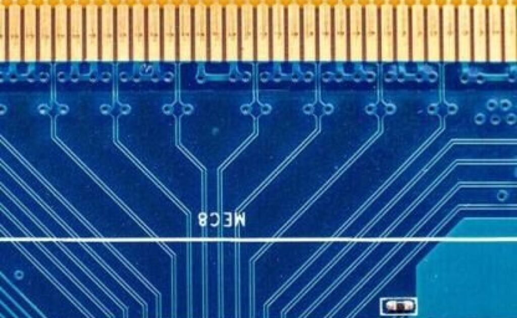
Remove the gold finger lead wire by beveling it for a neat gold finger.
A secondary etching process is usually required when dealing with the lead wire of gold fingers of different lengths. Simply speaking, the first etching process is etching the circuit of PCB, then using dry film or a peelable blue mask to cover the circuit area to plating the gold to the gold finger area by gold finger lead wire next are cover all other areas but the gold finger lead wire by dry film, at last, secondary etching the PCB gold finger lead wire.
Connect with us
Get an Instant Online Quote Today
Looking for reliable SMD assembly services? At ESPCBA, we’re your trusted partner for PCB fabrication, component sourcing, and electronic manufacturing. With over 16 years of experience, we’ve provided high-quality PCBs at competitive prices to over 1,000 customers worldwide. Our company is ISO9001:2015 certified and UL listed, and every product we deliver is 100% E-tested and inspected using AOI and X-ray to meet the highest standards. Get an instant quote from our sales team today, and let us handle the rest for you.
Frequently Asked Questions
PCB gold finger refers to the pads that insert into slots for electrical connection.
Repair methods vary; for example, tin removal may involve cleaning the solder, wiping with alcohol, and re-covering the gold finger with gold liquid.
PCB gold fingers typically range from 5 to 100 microns in thickness.
Gold fingers provide excellent conductivity, wear resistance, and corrosion protection.
Designs must ensure thicknesses from 0.25-1.3µm, 6-mil minimum distance between fingers, and proper chamfering for insertion.
The process involves electroplating, with dielectric nickel plating followed by gold plating. Non-gold plated pads are covered with tape before gold plating.
Typically, 30 to 50 micro-inches.
A bevel ensures secure and reliable connections between PCBs.
Gold fingers efficiently transfer power and data signals between PCBs, using gold's conductivity and durability.
PCBs requiring frequent plug-ins use hard gold plating for wear resistance, and no copper should be laid on the gold finger surface.
Gold resists oxidation and is highly conductive, making it ideal for connections.
The common IPC standards for gold fingers include IPC A-600 and IPC-6010.