
Printed circuit boards (PCBs) are the lifeblood of electronics today. But from smartphones to medical equipment, PCBs play a key role in making countless products functional. Have you ever asked how such complex boards are created? The PCB manufacturing process is a long, intricate process that takes a mere design and turns it into a working circuit board. In this blog, we’ll take a deep dive into the PCB manufacturing process, from design to production, and explore the steps involved in creating these essential components.
What is a PCB?
Let’s begin with the fundamentals before we move on to the manufacturing process. A PCB is a flat, non-conductive material board, usually fiber glass, having conductive paths etched or printed on its surface. The paths, referred to as traces, link several electronic components like resistors, capacitors, and ICs to create an entire circuit.
PCBs exist in different forms, such as single-sided, double-sided, and multi-layer boards, depending on the sophistication of the electronic product. Despite the form, the production involves a set of clearly defined stages to guarantee accuracy and dependability.
Step 1: PCB Design and Schematic Creation
The process of PCB production starts with design. Here, the designers and engineers prepare a design of the circuit board through specialized software like Altium Designer, Eagle, or KiCad. The design consists of two primary components:
1. Schematic Design
The schematic is an illustration of the circuit in graphical form, indicating how components are connected. It is a road map of the PCB layout and ensures all electrical connections are properly laid out.
2. PCB Layout
Once the schematic is complete, the following step is to design the PCB layout. This is a step of putting components onto the board and tracing the wires that route them between themselves. The layout has to take into account signal integrity, thermal design, and manufactureability.
In this step, designers also specify the dimensions, stack-up, and material requirements of the board. After the design is finalized, it is exported in Gerber file format, which the manufacturer then uses to create the PCB.
Step 2: Design Review and DFM Check
Before going into production, the design is reviewed in depth to make sure it complies with all the requirements. This involves a Design for Manufacturability (DFM) inspection, where the design is inspected for possible issues that may be encountered during production. Typical DFM considerations are:
Trace Width and Spacing: Make sure traces are of sufficient width to handle the current needed and sufficiently spaced so they do not short circuit.
Component Placement: Ensuring that components are positioned in a manner that facilitates effective assembly and soldering.
Drill Holes: Ensuring drill holes are properly sized and located for vias and component leads.
Issues found by the DFM check are resolved before going to the next step.
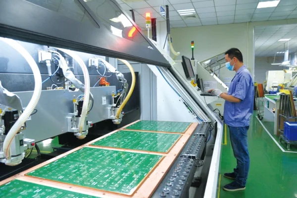
Step 3: PCB Fabrication
After finalizing the design, the manufacturing of the PCB starts. The actual board creation is done through some complex steps:
1. Material Selection
The substrate of PCBs most often consists of a laminate containing fibreglass and epoxy resin, a material referred to as FR-4. If the application demands high frequencies, Rogers or Teflon types of materials may be employed. The material’s selection is dependent on the end use of the board and expected performance.
2. Printing the Circuit Pattern
The circuit design is transferred to the board through the process of photolithography. A copper sheet is laminated onto the base material, followed by a deposit of photosensitive film (photoresist) over it. The Gerber files are inputted into software that generates the photomask, which covers the board. The UV light then shines on this assembly. Upon exposure, exposed parts of the photoresist turn hard, but unexposed areas are eroded, which results in the desired pattern of the circuit being left behind on the board.
3. Etching
The board is subsequently submerged in an etching bath, which dissolves away all the copper not protected by the photoresist, leaving traces defined by it. Following etching, any remaining photoresist is peeled off to reveal the pattern of copper circuits.
4. Drilling
There is drilling for vias (inter-layer connections) and leads of the components. It is performed by very precise CNC drills to ensure there are no inaccuracies.
5. Plating and Copper Deposition
The holes that have been drilled are copper-plated to make the electrical connections between the layers. Further layers of copper can be deposited to add thickness to the traces.
6. Solder Mask Application
A solder mask is applied on the board to shield the copper traces from oxidation and to avoid solder bridges upon assembly. Solder mask is normally green in colour, although other colours can also be used.
7. Silkscreen Printing
Component names, logos, and other labels are silkscreen printed onto the board. These facilitate assemblers in identifying components and their locations while assembling.
8. Surface Finish
A surface finish is used to coat exposed copper surfaces to prevent oxidation and enhance solderability. HASL (hot air solvent leveling), ENIG (electroless nickel immersion gold), and OSP (organic solventability preservative) are some of the most common surface finishes.
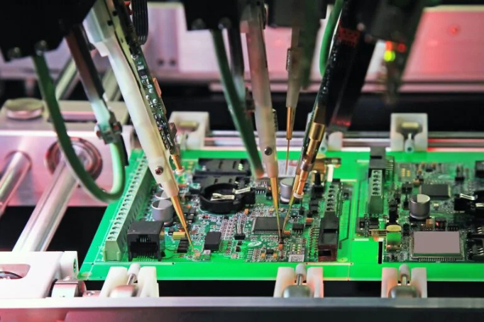
Step 4: PCB Assembly
After the board is manufactured, assembly is the next step. This includes mounting and soldering parts onto the board. There are two primary techniques of PCB assembly:
1. Through-Hole Technology (THT)
In THT, the leads of components are placed in holes drilled in the board and soldered on the other side of the board. This process is generally employed for large components or those needing high mechanical integrity.
2. Surface Mount Technology
In SMT, parts are mounted directly on the board surface and soldered in a reflow oven. SMT is the most prevalent method for contemporary PCBs because it enables smaller parts and increased density.
Assembly generally entails the following steps:
Solder Paste Application: Solder paste is deposited onto the board via a stencil.
Component Placement: Components are mounted on the board with pick-and-place machines.
Reflow Soldering: The board is sent through a reflow oven, where the solder paste is melted and creates a permanent bond.
Inspection and Testing: The assembled board is checked for defects and tested to make sure it works as designed.
Step 5: Quality Control and Testing
Quality control is an important aspect of the PCB manufacturing process. Every board is thoroughly tested to make sure it meets the specifications. Some common testing techniques are:
Visual Inspection: Verifying that the board does not have obvious defects like solder bridges, bent parts, or crushed traces.
Automated Optical Inspection (AOI): Utilizing cameras and algorithms to inspect for defects that can’t be detected by human vision.
Electrical Testing: Testing that the board works by measuring continuity, shorts, and opens.
Functional Testing: Applying conditions similar to how the board would be used to verify the board works.
Any flaws detected in the course of testing are fixed before shipping the boards to the customer.
Step 6: Final Packaging and Delivery
After all quality tests are successfully carried out, the boards are packed with utmost care so that they suffer no damage in transit. The boards can be shipped singly or in bundles depending on the needs of the customer.
Conclusion
The PCB fabrication process is an intricate and very exact process of turning a design into an operating circuit board. From the creation and manufacture of the board to its assembly and testing, each stage plays a key part in providing the ultimate product as per the best quality and dependability standards.
Here at ESPCBA, we specialize in offering premium PCB manufacturing services specifically designed for your unique needs. From a simple prototype to a sophisticated multi-layer board, our expert team is here to guide you every step of the way. Learn more about our services and how we can help you bring your designs to reality at our website (espcba.com).
By learning about the PCB manufacturing process, you can make the right choices and ensure that your projects are successful from the beginning to the end. So the next time you hold an electronic gadget in your hand, you will be able to appreciate the complex process behind it.