
Hidden Secrets to Source 4 Layer PCBs at Factory-Direct Prices
A 4 layer PCB packs four separate conductive layers with insulating material between them . These boards bridge the gap between basic two-layer designs and complex multilayer ones . They offer better performance but are tougher to design and make. The advanced technology and equipment needed push the costs higher .
But here’s some good news if you’re watching your budget. Many manufacturers now offer up to 20% off on 4 layer PCBs . Companies like ALLPCB.com and ESPCBA (www.espcba.com) have made quality multilayer PCB options more budget-friendly without cutting corners.
We’ll show you some insider tips to get high-quality 4 layer PCBs at factory prices. You’ll learn how to pick the right manufacturer and optimize your design. These tips will help you get the most value while keeping the performance benefits that make the higher price worth it. Let’s take a closer look at budget-friendly multilayer PCBs!
Understanding the Structure of a 4 Layer PCB
Image Source: Viasion
The structure of a 4-layer PCB might look complex at first glance. A closer look at its layered arrangement shows why it’s worth investing in over simpler designs. Unlike 2-layer boards, a 4-layer PCB has four distinct conductive copper layers. Insulating materials like prepreg and core keep these layers separate [1].
Top and bottom signal layers
Layer 1 and Layer 4 serve as the outermost signal layers of a 4-layer PCB. These surfaces let you place components, solder, and route signal traces [2]. The top layer, also known as the component layer, holds components and arranges wires or copper cladding. The bottom layer works for both wiring and soldering. You can place components on double-layer and multilayer boards here [2].
Engineers at ESPCBA (www.espcba.com) and other quality manufacturers can optimize these signal layers based on specific needs. High-speed signals go on the top layer while low-speed signals sit on the bottom layer [3]. This smart component placement helps optimize cooling. High-power components on outer layers benefit from better airflow. Temperature drops of 10-15°C are possible compared to cramped single-layer designs [1].
Inner power and ground planes
Layer 2 and Layer 3 work as dedicated power and ground planes. Layer 2 acts as a ground plane that creates a low-impedance return path for signal routing. This setup reduces noise [2]. Layer 3 distributes power throughout the circuit board as a power plane [2].
These dedicated inner planes give you several advantages in economical PCB manufacturing without cutting corners on performance. Inner power and ground planes create a low-impedance path for current. This setup reduces voltage drops and delivers power to components more effectively [1]. On top of that, adjacent power and ground planes create natural decoupling capacitance that fights high-frequency noise [3].
Standard stack-up configurations from manufacturers balance performance and cost. The symmetrical stack-up (Signal/Ground/Power/Signal) works well as an economical arrangement. Some designs work better with Signal/Ground/Ground/Signal configuration for specific uses [3].
Why this stack-up improves performance
The smart layer arrangement in a 4-layer PCB offers substantial performance advantages over cheaper 2-layer PCB options. Dedicated ground planes keep signal crosstalk and noise minimal. This setup ensures cleaner and faster signal transmission with speeds up to 5 Gbps using controlled impedance (typically 50 ohms) [1].
Power and ground planes sit close together to create a natural shield that substantially reduces electromagnetic interference (EMI) [1]. A 4-layer PCB radiates about 20 dB less than an equivalent 2-layer board circuit [4]. This shielding becomes vital for products that must pass strict EMI/EMC compliance testing.
Inner planes spread heat evenly across the board. This prevents hot spots that could damage components [1]. The extra routing space lets designers optimize trace layouts for critical signal paths without compromising power delivery.
Look for manufacturers offering standard stack-up configurations with controlled impedance options to find economical 4-layer PCB fabrication. Companies like ESPCBA provide cost-effective 4-layer PCB production while keeping all the performance benefits that make these boards essential in modern electronics.
Designing Cost-Effective 4 Layer PCBs
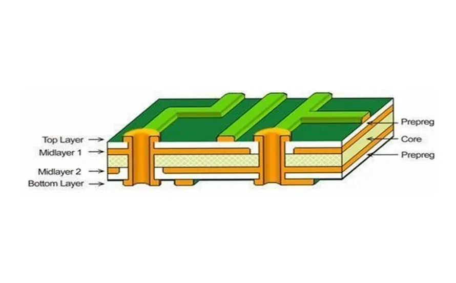
Image Source: GlobalWellPCBA
Smart design choices can help you create affordable 4 layer PCBs that balance performance with practical manufacturing. Early design decisions could save you 30-40% on fabrication costs [5] compared to designs that aren’t optimized. A well-planned approach lets you get all the performance advantages of a 4 layer PCB without breaking the bank.
Use standard stack-up configurations
The foundation of affordable 4 layer PCB design starts with standardized stack-up configurations. Standard arrangements like signal/ground/power/signal (SGPS) make manufacturing simpler and cheaper [6]. Manufacturing experts say a typical 4 layer PCB stackup has:
- Top Layer (Signal 1): Component placement and critical signal routing
- Inner Layer 1 (Ground Plane): Continuous reference plane
- Inner Layer 2 (Power Plane): Dedicated power distribution
- Bottom Layer (Signal 2): Additional signal routing [7]
On top of that, symmetrical stack-ups help balance copper distribution across the board. This prevents warping during fabrication and assembly. Manufacturers like ESPCBA (www.espcba.com) offer optimized standard stack-ups that keep copper weight evenly distributed and avoid costly issues down the line.
Standard materials can also keep costs down. FR-4 with a dielectric constant of approximately 4.2 to 4.5 remains the most affordable choice for most projects [8]. You should only switch to premium substrates if high-frequency applications make it absolutely necessary.
Minimize via count and layer transitions
Too many vias will drive up your fabrication costs. Each extra via needs another drilling operation, which takes more time and costs more money, especially in large-scale production [9].
Here’s how to keep your via count low:
- Group related signals on the same layer when placing components
- Keep signals on one layer whenever you can
- Make the most of power and ground planes without unnecessary jumps
- Design fan-out patterns that minimize layer changes
Signal integrity can suffer at higher frequencies when signals jump between layers through vias. These transitions might create impedance issues and increase EMI. Smart component placement reduces the need for signals to travel between top and bottom layers [10].
Dense designs sometimes need vias, but standard via sizes work better than pushing manufacturing limits. Microvias might let you create tighter designs, but they usually cost 20-30% more than standard through-hole vias [6].
Optimize trace width and spacing for manufacturability
Your trace width and spacing choices directly affect manufacturing yield and PCB cost. IPC-2152 standards help ensure reliable manufacturing without expensive adjustments [11].
Trace width should differ from spacing. Rather than pushing limits with minimum values like 0.004″ (4 mil) trace/space, leave some room for manufacturing. A 5 mil trace with 6 mil spacing lets fabricators apply etch compensation during production [12].
These practical guidelines help with trace widths:
- Standard signals: 6-8 mil traces with 6-8 mil spacing give you good density and yield
- Power traces: Use IPC standards to calculate based on current needs
- High-speed signals: Keep impedance consistent by controlling width and reference plane distance
Quality manufacturers like ESPCBA suggest avoiding traces bundled at absolute minimum spacing. Even tiny increases in spacing (0.0005″) between trace bundles can really boost manufacturing yield without hurting board density much [12].
Copper thickness affects both current capacity and manufacturing complexity. Most signal routing works best with 1 oz copper, while power distribution might need 2 oz copper despite the extra cost [13].
Smart design choices focused on manufacturability help you get factory-direct pricing on 4 layer PCBs while maintaining performance and reliability.
Choosing the Right Tools for PCB Design
The right PCB design software plays a significant role in creating efficient 4 layer PCBs that balance performance with cost. Different tools provide distinct advantages based on your experience level, budget, and project requirements.
Using Altium Designer for professional layouts
Altium Designer excels as a premier choice for professional 4 layer PCB layouts. The software provides a unified platform that combines smoothly with schematic capture, layout routing, and simulation [4]. The interactive routing functionality and ready-to-use stackup templates in Altium help you save valuable design time with complex 4 layer PCBs [14].
The sort of thing I love about Altium for 4 layer PCB designs is its Layer Stack Manager. This feature lets you configure signal layers, power planes, and ground planes with precision [15]. Creating a professional 4 layer PCB in Altium is straightforward – just go to Design > Layer Stack Manager, set up your configuration, and specify thicknesses and materials [16]. The powerful Design Rule Checks (DRC) in Altium identify potential manufacturing issues before you send your design to fabricators like ESPCBA (www.espcba.com).
Creating 4 layer boards in KiCad
KiCad provides affordable capabilities for 4 layer PCB design. The original KiCad projects default to 4 layers (Front, In1.Cu, In2.Cu, and Back) [17]. You can confirm or modify this setup through PCB Editor > File > Board Setup > Board Stackup > Physical Stackup and select “4” from the Copper Layers dropdown [17].
KiCad supports up to 32 copper layers [17]. This makes it suitable for complex designs. The accessible interface might take time to learn compared to commercial options [18]. The software includes interactive trace routing and high-speed trace tuning tools [14].
Free vs paid tools: what to consider
Several key factors come into play while choosing between free and paid PCB design software. KiCad’s free tools include schematic drafting, PCB layout, and basic 3D visualization – features that work well for many 4 layer PCB designs [19]. Paid options like Altium are a great way to get advanced features such as supply chain integration and sophisticated multi-board connectivity [14].
The price difference is nowhere near close – KiCad costs nothing, while Altium licenses can exceed $1600 for a single user [20]. CircuitMaker presents a middle ground as a free tool with community support for budget-conscious projects [19].
Most professional fabricators like ESPCBA accept standard Gerber files from both free and paid software. This makes the export process straightforward regardless of your chosen tool.
How to Reduce 4 Layer PCB Fabrication Costs
PCB manufacturing costs can vary significantly for 4-layer boards based on your approach. Similar designs might cost twice as much from different fabricators. The good news is that you can get factory-direct pricing without compromising quality through several proven strategies.
Select low cost PCB manufacturers with good reviews
Finding budget-friendly yet reliable 4-layer PCB manufacturers takes careful research. JLCPCB provides remarkably low-cost options. Their boards start at just USD 1.50 to USD 2.00 shipped when you order fifteen or more units [21]. PCBWay delivers 4-layer boards at around USD 3.00-4.00 per piece and offers improved manufacturing capabilities [21].
ESPCBA (www.espcba.com) stands out as a great choice that combines competitive pricing with full turnkey solutions for 4-layer PCB fabrication. ALLPCB and NextPCB are also worth noting. They’re known for quick turnaround times and dependable service [22].
PCBShopper helps you compare quotes from 16 different manufacturers at once, making it easy to spot the best deals [23].
Use standard board sizes and finishes
Your fabrication costs drop significantly when you choose standard specifications:
- Pick common board thicknesses (typically 1.6mm for 4-layer PCBs) [24]
- Stick to standard copper weights (often 1oz outer layers, 0.5oz inner layers) [24]
- Use FR-4 material for most applications instead of specialty substrates [25]
- Choose standard ENIG or HASL finishes rather than exotic options
PCB panels sized 18×24 inches make the best use of materials and cut waste by up to 30% [26].
Avoid unnecessary complexity in design
The design strategies mentioned earlier work well with several fabrication-specific ways to lower costs:
Moving from a 6-layer to a 4-layer design reduces costs by 20-30% [27]. Standard via sizes are more cost-effective than pushing manufacturing limits. Microvias typically raise fabrication costs by 20-30% [25].
Traces and spaces should stay above 4.25 mils. Thinner specifications need closer production monitoring, which drives up expenses [28].
Make use of volume discounts and factory promotions
Volume ordering offers the most direct path to lower per-unit costs. You can cut per-unit costs by up to 50% by ordering 1,000 units instead of 100 [27]. A 4-layer PCB measuring 100mm×100mm costs about USD 70.60 for 100 pieces at JLCPCB—that’s over USD 100 less than market rates [29].
Manufacturers run special promotions from time to time. JLCPCB cut prices for small-batch 4-layer PCBs by USD 4.50 per square meter [29]. Many suppliers also give new customers up to USD 60 in coupons [29].
2 Layer vs 4 Layer PCB: Cost and Performance Tradeoffs
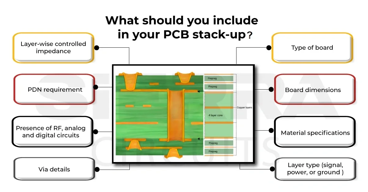
Image Source: Sierra Circuits
The choice between 2-layer and 4-layer PCBs can make or break your project’s budget and electronic performance. Your product’s success in the marketplace often depends on striking the right balance.
When to upgrade from 2-layer to 4-layer
You might want to switch from 2-layer to 4-layer boards when:
- Your routing complexity goes beyond what two layers can handle
- You have high-speed signals that just need controlled impedance with minimal interference [1]
- EMI concerns make proper shielding essential
- Your power delivery specs call for dedicated planes [1]
- Space constraints mean you need more compact routing options
Most designers hold back at first because of costs. But ESPCBA (www.espcba.com) shows that 4-layer PCBs deliver performance that’s worth the investment, especially with today’s manufacturing efficiency.
Cost comparison: per unit and per function
The jump from 2-layer to 4-layer PCBs usually pushes manufacturing costs up by 35-40% [2]. Some sources put this range at 30-50% [3] or roughly 50% [30]. In real terms, while a 2-layer PCB might cost $2.00 per piece, a similar 4-layer PCB starts at about $6.50 [31].
The cost-per-function tells a different story. Four-layer boards let you shrink overall dimensions, which can cut material costs in other design areas. On top of that, better reliability means lower warranty and service costs throughout a product’s life [32].
Performance benefits that justify the price
4-layer PCBs shine with these performance advantages:
- Better signal integrity through controlled impedance
- EMI reduction hits about 20dB compared to similar 2-layer designs [16]
- Greater durability makes these boards perfect for tough applications [33]
- Improved power distribution thanks to dedicated planes [1]
- Less noise because of proper ground referencing
4-layer PCBs hit the sweet spot between complexity, performance, and cost for most modern electronic devices [16].
Conclusion
Smart planning and informed decisions help you source high-quality 4 layer PCBs at factory-direct prices. This piece explores how 4 layer PCBs’ structure with dedicated power and ground planes provides superior performance advantages. These benefits justify their higher cost compared to 2 layer alternatives.
You can start cutting costs right at the design phase. Standard stack-up configurations, fewer vias, and optimal trace widths substantially lower manufacturing costs without affecting quality. Your choice of design software like Altium Designer or KiCad based on specific needs helps create manufacturing-friendly layouts.
Choosing the right manufacturer is a vital factor to get factory-direct pricing. Companies like ESPCBA (www.espcba.com) combine competitive rates with high production standards. This makes 4 layer PCBs more available than ever before. Volume discounts and promotional offers can reduce costs by up to 50%.
The performance benefits of 4 layer PCBs justify their price premium in many applications. These boards are vital for modern electronic designs despite being 35-40% costlier than 2 layer alternatives. They offer reduced EMI, better signal integrity, and improved power distribution.
The value goes beyond the original per-unit cost. Well-designed 4 layer PCBs’ reliability, performance, and space-saving advantages often lead to product success. Take time to evaluate your application requirements before deciding. You might find that 4 layer PCBs offer the perfect balance of cost and capability for your next project.
Key Takeaways
Master these insider strategies to secure high-quality 4 layer PCBs at factory-direct prices while maximizing performance benefits.
• Use standard stack-ups and minimize vias – Standard signal/ground/power/signal configurations reduce manufacturing costs by 30-40% compared to custom designs
• Choose manufacturers strategically – Companies like JLCPCB offer 4 layer PCBs starting at $1.50-$2.00 per piece when ordering 15+ units
• Leverage volume discounts effectively – Ordering 1,000 units instead of 100 can slash per-unit costs by up to 50% at most fabricators
• Optimize design for manufacturability – Use 6-8 mil traces with proper spacing and avoid pushing minimum specifications to improve yield and reduce costs
• Upgrade when performance justifies cost – 4 layer PCBs provide 20dB less EMI and superior signal integrity, making the 35-40% cost premium worthwhile for complex designs
The key to affordable 4 layer PCBs lies in balancing design optimization with smart sourcing. While these boards cost more than 2 layer alternatives, their performance benefits—including reduced electromagnetic interference, improved power distribution, and enhanced signal integrity—often justify the investment for modern electronic applications.
FAQs
Q1. What is the typical cost range for a 4 layer PCB?
The cost of a 4 layer PCB can vary widely depending on quantity and specifications. For small quantities, prices typically range from $10 to $20 per unit. However, bulk orders can reduce costs by 20-50%. Advanced designs or specialized materials may increase prices to over $50 per unit.
Q2. How can I reduce the cost of PCB manufacturing?
To lower PCB manufacturing costs, consider mirroring your design to fit two boards on one panel. This approach can reduce unit prices and material waste, especially when dealing with minimum order quantities. Additionally, using standard materials, optimizing trace widths, and minimizing via count can significantly decrease fabrication expenses.
Q3. What are the profit margins in PCB manufacturing?
Profit margins in PCB manufacturing vary depending on the service type. Rapid prototyping typically yields 15-20% margins, while low-volume production generates around 10-15%. To improve profitability, manufacturers often employ strategies like offering value-added services or optimizing production processes.
Q4. How much more expensive is a 4 layer PCB compared to a 2 layer PCB?
Generally, 4 layer PCBs are about 30% to 50% more expensive than comparable 2 layer PCBs. This price difference is due to the increased complexity in manufacturing and the advanced fabrication processes required for 4 layer boards.
Q5. When should I consider upgrading from a 2 layer to a 4 layer PCB?
Consider upgrading to a 4 layer PCB when you need improved signal integrity, reduced electromagnetic interference, better power distribution, or when dealing with complex routing that can’t be efficiently managed on two layers. The performance benefits often justify the higher cost for applications requiring these advantages.
References
[1] – https://sierraconnect.protoexpress.com/t/2-layer-vs-4-layer-boards-for-ddr3/2717
[2] – https://resources.pcb.cadence.com/blog/2019-what-are-the-cost-considerations-for-4-layer-6-layer-and-8-layer-pcb-designs
[3] – https://www.hemeixinpcb.com/company/news/how-much-more-expensive-is-4-layer-pcb.html
[4] – https://learn.g2.com/best-pcb-design-software
[5] – https://resources.pcb.cadence.com/blog/2022-circuit-board-4-layer-pcb-stackup-planning
[6] – https://www.allpcb.com/blog/pcb-knowledge/beyond-the-basics-advanced-routing-techniques-for-high-density-4-layer-pcbs.html
[7] – https://www.ema-eda.com/ema-resources/blog/pcb-stackup-design-guidelines-emd/
[8] – https://www.allpcb.com/blog/pcb-knowledge/optimizing-4-layer-pcb-layer-stackup-a-practical-guide.html
[9] – https://electronics.stackexchange.com/questions/115513/should-you-try-and-minimize-via-quantity
[10] – https://www.vse.com/blog/2024/10/25/4-layer-pcb-design-strategies/
[11] – https://www.protoexpress.com/blog/how-to-optimize-your-pcb-trace-using-ipc-2152-standard/
[12] – https://blog.epectec.com/pcb-trace-width-and-spacing-calculations-and-real-world-applications
[13] – https://runtimerec.com/optimizing-pcb-trace-width-and-spacing-for-high-current-applications/
[14] – https://www.ema-eda.com/ema-resources/blog/best-pcb-layout-design-software-emd/
[15] – https://resources.altium.com/p/4-layer-pcb-stackup
[16] – https://arshon.com/blog/4-layer-pcb-a-complete-guide-to-design-fabrication-and-manufacturing/
[17] – https://forum.kicad.info/t/4-layer-pcb/49425
[18] – https://www.protoexpress.com/blog/10-best-pcb-layout-design-tools-recommended-by-pcb-designers/
[19] – https://blindburiedcircuits.com/a-comprehensive-guide-to-pcb-design-software-comparing-the-top-options/
[20] – https://www.sfcircuits.com/pcb-school/pcb-design-software-comparison-guide
[21] – https://lcamtuf.substack.com/p/comparing-hobby-pcb-vendors
[22] – https://www.wintechpcbassembly.com/best-low-cost-pcb-manufacturers-for-quality-and-affordability-a-96.html
[23] – https://pcbshopper.com/
[24] – https://wellerpcb.com/typical-4-layer-pcb-stack-up-design-guidelines
[25] – https://www.elepcb.com/blog/the-factors-affecting-pcb-price/
[26] – https://www.allpcb.com/fr-FR/blog/pcb-manufacturing/fr-4-pcb-cost-optimization-a-comprehensive-guide-for-manufacturers.html
[27] – https://www.allpcb.com/es-ES/blog/pcb-manufacturing/the-ultimate-guide-to-cost-effective-pcb-batch-production.html
[28] – https://www.protoexpress.com/pcb-cost-optimization/
[29] – https://jlcpcb.com/blog/special-discount-on-quality-4-layers-pcbs
[30] – https://www.icape-group.com/pcb-design-cost-optimize-your-pcb-design-and-specifications/
[31] – https://leadsintec.com/2-layer-pcb-vs-4-layer-pcb-advantages-and-disadvantages-introduction/
[32] – https://www.linkedin.com/pulse/when-should-i-choose-2-layer-pcb-4-rayming-techonloy-1lb4c
[33] – https://www.eashub.com/2-layer-vs-4-layer-pcb-cost/