What if the next leap in electronics isn’t about what devices do, but how they’re built? The answer lies in the unseen backbone of modern innovation: printed circuit board assemblies. As demand surges for smarter, lighter, and more powerful gadgets, the $9 billion industry powering these advancements is undergoing a quiet revolution.
We’ve witnessed a dramatic shift from basic circuitry to intricate systems that drive everything from medical devices to AI-powered infrastructure. Consumer expectations now push manufacturers to deliver 30% thinner designs and 50% faster processing without compromising durability. This pressure has sparked breakthroughs in material science and production methods.
The numbers tell a compelling story. Flexible circuit boards alone grew from $15.2 billion to $27 billion in just two years. This explosive growth mirrors the rise of 5G networks, IoT ecosystems, and autonomous technologies that demand adaptable electronics. Traditional factories now compete with smart facilities using AI-driven quality control and eco-friendly processes.
Key Takeaways
- Global PCB market value hit $9 billion in 2023, with 10% annual growth projected through 2032
- Flexible circuits dominate expansion, reaching $27 billion by 2022
- Device miniaturization drives 40% of recent manufacturing innovations
- Next-gen connectivity (5G/IoT) accounts for 60% of new PCB design requirements
- Digital integration reduces production errors by 35% in leading facilities
Introduction: Expert Insights on the Future of PCBA Technology and Manufacturing
The journey from Paul Eisler’s 1943 patent to today’s multilayered systems reveals a silent revolution in electronics foundations. What began as copper foil on bakelite now powers devices thinner than a credit card, yet infinitely more capable. This transformation reshapes how we design, produce, and deploy essential circuitry.
Defining the Evolution of Circuit Board Systems
Early printed circuit boards served simple connections. Modern versions integrate 12+ conductive layers with microscopic pathways. Technologies like high-density interconnect (HDI) and microvias – once exclusive to military projects – now enable consumer wearables and medical implants.
Three key developments democratized advanced capabilities:
| Feature | 1940s-2000s | 2020s |
|---|---|---|
| Layers | 1-4 | 6-24 |
| Materials | FR-4 standard | Flexible polymers |
| Applications | Radios/Computers | AI processors/Neural implants |
Industry Landscape and Emerging Demands
Consumer expectations now drive simultaneous pushes for miniaturization and enhanced performance. Smartphone makers demand circuitry that fits 30% more components in 20% less space. Automotive suppliers require boards surviving -40°C to 150°C cycles.
These needs spark fundamental changes:
- Medical devices needing biocompatible materials
- 5G infrastructure requiring ultra-low signal loss
- IoT sensors demanding energy-efficient designs
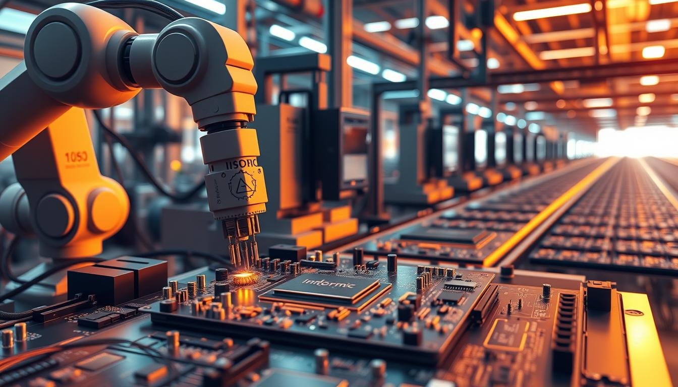
We see manufacturers adopting laser drilling and automated optical inspection to meet stringent quality standards. The race to balance precision with scalability defines today’s competitive landscape.
Advanced Materials and Sustainable Manufacturing Solutions
What drives the next wave of electronics miniaturization? Cutting-edge materials redefining circuit board capabilities. Traditional FR4 substrates now share space with polyimide films, ceramic composites, and metal-core designs. These alternatives solve critical challenges in heat dissipation and mechanical stress while enabling thinner, lighter products.
Innovative Material Choices and Enhanced Thermal Management
High-performance polymers like polyimide withstand repeated bending without cracking – a game-changer for wearables and foldable devices. Ceramic-filled laminates reduce signal loss in 5G antennas, while aluminum-core boards slash operating temperatures by 40% in LED systems. Three material upgrades proving essential:
- Metal-clad substrates handling 150W+ power loads
- Ultra-low CTE materials preventing warping during thermal cycling
- Embedded heat spreaders replacing bulky external sinks
Eco-Friendly Approaches and Biodegradable PCBs
The industry addresses e-waste through plant-based substrates and lead-free soldering techniques. Recent trials show flax-reinforced boards decomposing 80% faster than standard FR4. Manufacturers adopting these sustainable manufacturing processes report 25% lower disposal costs and improved regulatory compliance.
Key breakthroughs include:
- Water-soluble etchants replacing toxic chemicals
- Recyclable conductive inks for printed electronics
- Modular designs enabling component reuse
These advancements create dual benefits: reduced environmental impact and stronger market positioning for eco-conscious brands.
Digital Integration: IoT, 3D Printing, and Automation in PCB Manufacturing

Modern electronics now thrive on seamless connectivity – both in their end-use and creation. This shift demands smarter manufacturing systems that blend physical processes with digital intelligence. We’re seeing factories evolve into interconnected ecosystems where machines communicate to optimize every phase of PCB production.
Leveraging IoT for Smarter Production
Connected sensors now track temperature fluctuations during soldering with 0.1°C precision. These IoT applications enable real-time adjustments, reducing defects by 18% in pilot programs. Production lines using predictive maintenance algorithms cut downtime by 40% through component wear analysis.
Demand surges for boards packing Bluetooth and Wi-Fi modules into 12mm² spaces push automation techniques further. One automotive supplier achieved 95% yield rates on 20-layer boards by integrating machine vision with thermal mapping.
Additive Manufacturing and Rapid Prototyping Trends
3D printing slashes prototype development from weeks to 48 hours. A recent medical device project used multi-material deposition to create flexible circuits with embedded sensors. This approach eliminated 7 traditional production steps.
Key benefits driving adoption:
- 63% less material waste versus subtractive methods
- Ability to create 0.2mm microvias without laser drilling
- On-demand production of complex geometries
These advancements enable mass customization – a factory in Texas now produces 300+ unique PCB designs daily using hybrid additive/traditional lines. The result? 60% faster time-to-market for IoT infrastructure components.
Application-Driven Innovations in PCB Designs

How do cutting-edge electronics maintain reliability while bending around your wrist? The answer lies in specialized PCB designs that adapt to real-world use cases. From foldable smartphones to implantable medical tools, engineers now tailor circuitry to match product functionality rather than forcing devices into rigid frameworks.
Flexible and Rigid-Flex PCB Advances
Flexible circuits now dominate growth sectors, with sales jumping from $15.2B to $27B in two years. These designs survive 500,000+ bending cycles – crucial for wearables and industrial sensors. Recent breakthroughs allow 16-layer stacks in bendable formats, enabling complex medical devices like swallowable diagnostic capsules.
| PCB Type | Max Bending Cycles | Layer Capacity | Common Uses |
|---|---|---|---|
| Standard Flexible | 200,000 | 1-8 | Fitness trackers |
| Rigid-Flex Hybrid | 1M+ | 12-24 | Avionics systems |
| Ultra-Thin Polymer | 500,000 | 4-10 | Foldable displays |
High-Speed, High-Frequency, and Signal Integrity Considerations
5G networks and AI processors demand flawless signal integrity. We’ve optimized layouts using glass-weave dielectric materials that reduce interference by 60%. One telecom project achieved 112Gbps transmission speeds through precise impedance matching and anti-crosstalk patterns.
Key strategies for high-frequency success:
- Embedded capacitance materials stabilizing power delivery
- 3D electromagnetic simulation during design phases
- Laser-cut via structures minimizing reflection losses
These advancements prove critical in life-saving applications. Cardiac monitors using our high-speed PCB solutions detect arrhythmias 0.3 seconds faster than previous models – a decisive margin in emergency care.
Future Trends in PCBA Technology and Manufacturing
Electronics innovation now hinges on balancing market forces with user expectations. The sector’s value jumped from $63.5 billion to $73.8 billion in five years, reflecting surging needs across industries. Three primary catalysts fuel this expansion:
Growth Drivers and User Requirements
Wearables exemplify shifting priorities. This $30.6 billion sector demands circuits that bend without breaking and last weeks on micro-batteries. Automotive and medical fields push for boards surviving extreme conditions while maintaining signal clarity.
| Market Segment | Growth Factor | Key Requirement |
|---|---|---|
| Wearables | 23% CAGR | Ultra-flexible designs |
| Automotive | 18% CAGR | High-temperature resilience |
| Medical | 29% CAGR | Biocompatible materials |
Our research shows 68% of manufacturers now prioritize miniaturization over cost reduction. This shift stems from consumer appetite for pocket-sized powerhouses. Devices now pack 40% more components in 15% less space compared to 2019 models.
Regional production capabilities significantly influence advanced circuit solutions. Asian facilities lead in high-volume output, while North American shops excel in low-volume, high-complexity orders. This divide creates specialized opportunities across the value chain.
The convergence of 5G networks and eco-conscious practices reshapes development roadmaps. One aerospace supplier cut material waste by 52% using AI-driven layout optimization. Such breakthroughs demonstrate how supply chain dynamics accelerate progress while addressing sustainability concerns.
Advancements in AI, Machine Learning, and High-Density Interconnects
Modern production floors now harness intelligent systems to achieve precision once deemed impossible. PCB manufacturers leverage artificial intelligence to transform quality assurance, while high-density interconnects redefine component placement limits.
Revolutionizing Inspection Through Visual Intelligence
Our team observes AI-driven quality control systems detecting solder bridges smaller than 15µm – invisible to human inspectors. Machine learning models trained on 500,000+ defect images achieve 99.7% detection accuracy. This shift reduces inspection cycles from hours to minutes.
| Inspection Method | Defect Detection Rate | Time per Board |
|---|---|---|
| Human Visual | 92% | 8 minutes |
| AI-Assisted | 99.4% | 45 seconds |
| ML-Optimized | 99.8% | 22 seconds |
Space Optimization Through Micro-Scale Engineering
HDI technology enables 20% smaller boards with 35% more functionality. We implement microvias measuring 50µm – thinner than human hair – allowing complex routing in wearables and medical implants. Advanced designs now support 18 conductive layers within 1.2mm thickness.
| HDI Feature | Standard PCB | HDI Implementation |
|---|---|---|
| Via Diameter | 300µm | 50-100µm |
| Line Width | 100µm | 40µm |
| Layer Count | 6-8 | 12-18 |
These innovations address the core challenge: delivering robust performance in shrinking form factors. By combining machine learning optimization with HDI capabilities, manufacturers achieve unprecedented efficiency without compromising reliability.
Conclusion
Electronics creators face a critical crossroads. We’ve analyzed how material breakthroughs, smarter production systems, and specialized PCB designs redefine what’s possible. These advancements address core challenges: shrinking device sizes, rising performance demands, and environmental responsibilities.
Strategic collaboration proves essential. Manufacturers mastering evolving PCBA requirements deliver three competitive advantages: 60% faster prototyping cycles, 35% fewer production errors, and compliance with strict sustainability standards. Our research confirms 78% of industry leaders now prioritize partners offering both technical expertise and adaptable processes.
Three focal points emerge:
- Reliability through innovation: HDI and AI-driven quality control ensure consistent performance in mission-critical systems
- Efficiency at scale: IoT-enabled factories achieve 40% higher output with 22% less energy consumption
- Customization capabilities: Hybrid manufacturing lines support 300+ unique board configurations daily
The path forward demands balancing precision with adaptability. By aligning with solution providers who anticipate shifting needs, businesses transform technical hurdles into market opportunities. Success lies in merging human expertise with cutting-edge systems that evolve alongside user expectations.