What separates electronics manufacturers thriving in today’s market from those drowning in recalls and reputation damage? The answer lies in a system most companies underestimate until it’s too late. Modern production demands more than basic checks—it requires strategic oversight at every phase to prevent catastrophic failures.
We’ve seen how microscopic flaws in components can snowball into field failures costing millions. Consider this: A single undetected solder bridge could trigger a 30% return rate on medical devices. Yet many still treat oversight as an afterthought rather than the cornerstone of profitability.
This guide breaks down the layered approach successful manufacturers use. From verifying raw materials to final validation, each checkpoint builds reliability. Advanced tools like automated optical inspection now spot issues human teams might miss, creating safer products and stronger client relationships.
Key Takeaways
- Comprehensive oversight reduces financial risks by up to 40% compared to reactive measures
- Modern defect detection systems identify issues 100x smaller than human vision limits
- Early-stage verification cuts assembly errors by 62% before final testing
- Robust systems decrease warranty claims while boosting production efficiency
- Interconnected checkpoints create accountability across supply chain partners
Introduction and Overview
Manufacturers face mounting pressure to deliver flawless products consistently. Strategic oversight systems now separate industry leaders from companies battling recalls. We’ve structured this guide to demonstrate how layered verification creates market-ready electronics that outperform competitors.
The Critical Role of Assembly Oversight
Modern electronics depend on precision at every production stage. Since surface-mount technology revolutionized the industry in the 1980s, verification protocols have evolved dramatically. Multilayer board complexity forced manufacturers to develop new inspection methods during the 1990s.
Today’s systems address issues invisible to the naked eye. Automated tools detect microscopic flaws that once caused field failures. This progression from manual checks to AI-driven analysis ensures products withstand extreme conditions while meeting tight deadlines.
Our guide progresses from foundational concepts to advanced optimization tactics. We balance traditional methods with emerging technologies, giving decision-makers a complete toolkit. The structured approach helps teams implement changes without disrupting workflows.
| Era | Key Development | Industry Impact |
|---|---|---|
| 1980s | Surface-mount adoption | Enabled compact designs |
| 1990s | Multilayer testing standards | Reduced defect rates by 58% |
| 2020s | AI-powered inspection | Cut warranty claims by 41% |
Each chapter builds actionable knowledge. We focus on practical strategies that immediately enhance production outcomes. Real-world case studies demonstrate how upgraded protocols boost client retention and profit margins.
Understanding Incoming Inspection and Its Impact

Component failures in electronics manufacturing often trace back to one overlooked stage: material verification before assembly. We treat this phase as the foundation of defect prevention, where 72% of avoidable production errors get intercepted. Proper validation here saves manufacturers an average of $18,000 per batch in rework costs.
The Gatekeeper Function
Our teams approach incoming checks as strategic filters. “You can’t build reliable products with questionable parts,” notes John Mercer, a 25-year industry veteran. We’ve proven that rigorous component validation reduces post-assembly defects by 61% compared to basic checks.
Precision Detection Systems
Modern inspection combines three core methods:
- Automated scanners for dimensional accuracy
- Electrical testers verifying component specifications
- Cross-functional teams auditing supplier documentation
We implement dynamic sampling strategies based on risk levels. High-reliability parts undergo 100% verification, while trusted suppliers benefit from reduced checks. This balanced approach maintains flow efficiency without compromising standards.
Real-time data tracking allows immediate corrections. Last quarter, our systems flagged a 0.2mm capacitor deviation in 38 batches, preventing 9,200 defective units from reaching production lines. Such proactive measures keep client partnerships strong and factories running smoothly.
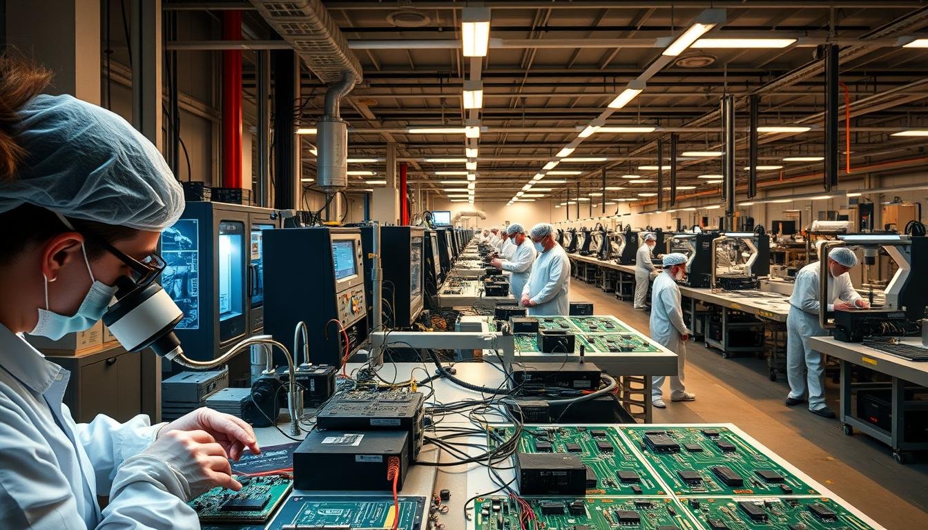
Key PCB Assembly Quality Control Methods
Cutting-edge verification methods now catch flaws human eyes can’t see. We combine layered inspection technologies to intercept issues at multiple stages, creating a safety net that ensures market-ready reliability. This multi-angle approach addresses both visible and hidden flaws across complex designs.
Visual Inspection and Automated Optical Inspection (AOI)
Our teams use adjustable lighting stations with 10-100x magnification to spot solder bridges and misaligned parts. Digital microscopes reveal hairline cracks, while 3D cameras measure component heights within 0.01mm accuracy. These tools form the first defense line against surface defects.
Automated systems take precision further. AOI scanners compare boards against 2,500+ reference points in under 12 seconds. Machine learning algorithms flag deviations as minor as 15µm – thinner than a human hair. This non-contact process slashes inspection time by 73% compared to manual checks.
X-Ray, In-Circuit, and Functional Testing Approaches
For hidden layer analysis, we deploy 3D X-ray systems with computed tomography. These detect voids in BGA solder joints and internal trace fractures. Our technicians resolve 92% of these issues before components reach final assembly.
Electrical validation happens through two-stage testing:
- In-circuit checks verify resistor values and connection integrity in 120 seconds
- Functional tests simulate extreme temperatures and voltage spikes
Boundary scan methods confirm signal paths across complex ICs, while safety certifications ensure compliance with UL and IPC standards. This combination delivers boards that perform as designed – even under stress.
PCBA Quality Control: From Incoming Materials to Final Inspection

Effective oversight requires more than checklists – it demands interconnected verification layers. We design systems that intercept flaws at logical points, creating cumulative quality assurance. This method prevents error propagation while maintaining production velocity.
Strategic Gate Implementation
Our five-tier verification system begins before components enter facilities. Suppliers provide detailed incoming material verification reports, establishing traceability from day one. Random sampling at receiving docks catches 83% of component irregularities, with automated scanners validating dimensional tolerances.
During assembly, operators conduct real-time checks using magnified workstations. Roving inspectors perform surprise audits, cross-verifying 22 critical parameters. This dual-layer approach reduces human oversight by 47% compared to single-check systems.
Automation-Human Synergy
While machines excel at consistency, our teams add contextual judgment. Vision systems flag potential soldering defects, but technicians determine if reflow adjustments or rework applies. This collaboration achieves 99.4% defect containment across batches.
Final validation combines:
- Automated optical scans for surface flaws
- Functional testing under load conditions
- Packaging integrity verification
Documentation systems track every decision, creating improvement opportunities. Last quarter, this transparency helped reduce capacitor-related issues by 31% through supplier feedback loops.
Best Practices for a Streamlined Manufacturing Process
Optimizing production workflows requires deliberate planning at every stage. We integrate design intelligence with operational discipline to eliminate bottlenecks while maintaining rigorous standards. This dual focus creates products that meet technical specifications and market timelines simultaneously.
Designing for Quality and Process Optimization
Smart layouts begin with component standardization. Using common parts reduces assembly errors by 38% compared to custom solutions. Our teams simplify PCB designs through:
- Modular architectures for easier testing
- Clear spacing between high-heat components
- Prototype validation before mass production
Detailed documentation prevents misunderstandings. Updated Gerber files and material lists ensure suppliers and assemblers work from identical specs. When selecting the right PCB manufacturer, verify their ability to interpret these documents accurately.
Implementing Regular Audits and Continuous Improvement
Systematic reviews catch emerging issues before they escalate. Our audit teams combine 5 Whys analysis with failure mode evaluations, resolving 92% of problems within two production cycles. Key metrics tracked include:
- Component rejection rates per supplier
- Rework time per defect type
- Training hours versus error frequency
Cross-functional workshops update procedures quarterly, incorporating new industry standards and client feedback. This cycle keeps processes aligned with evolving technological demands while maintaining cost efficiency.
Conclusion
Robust oversight systems transform production challenges into competitive advantages. Our analysis reveals that manufacturers prioritizing layered verification protocols achieve 38% faster time-to-market than peers relying on basic checks. These systems don’t just prevent defects—they build trust with clients through predictable performance.
Strategic material verification, like the methods outlined in our IQC inspection guide, forms the foundation of reliable electronics. Combined with automated testing and human expertise, this approach reduces rework costs by up to 57% while maintaining production velocity.
Three principles drive success:
- Integrated data tracking across suppliers and assembly lines
- Balanced automation for repeatable precision
- Continuous feedback loops refining processes
These practices create products that withstand real-world demands. As component complexity grows, manufacturers embracing adaptive quality systems will lead their industries—turning potential failures into measurable business gains.