Imagine this: your team just approved a new PCB design after months of development. But hidden flaws emerge during final quality checks, delaying shipments and frustrating clients. Could your testing strategy be the silent profit killer?
Modern electronics manufacturing demands precision without compromising speed or budget. Two automated approaches dominate today’s industry—traditional bed-of-nails systems and agile robotic testers. Each method solves critical challenges but operates under different economic and technical rules.
We’ve seen projects stumble when teams prioritize familiarity over data-driven analysis. Upfront costs for custom fixtures might seem logical for high-volume runs. But what happens when design changes demand hardware revisions? Conversely, flexible probe systems eliminate tooling expenses but require longer test cycles. The balance shifts dramatically based on production quantities and design complexity.
Key Takeaways
- Production volume determines which method delivers better ROI
- Fixture costs impact budget viability for small batches
- Frequent design updates favor systems needing no physical adapters
- Test coverage varies between component-level and network analysis
- Lead times differ significantly during initial setup phases
Through years of optimizing validation processes, we’ve identified four decision pillars: per-unit economics, defect detection scope, development timelines, and adaptability to revisions. Let’s unpack how these factors shape outcomes across product lifecycles.
Overview of PCB Testing Methods
Modern electronics manufacturers face critical choices when validating assembled boards. Two automated approaches dominate production floors today, each offering unique benefits for verifying printed circuit integrity. Let’s examine how these systems work and where they excel.
Defining ICT and Its Process
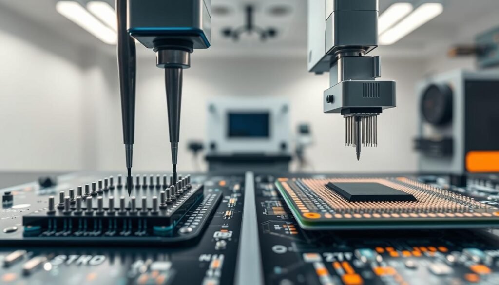
The first method employs a bed nails fixture housing hundreds of spring-loaded contacts. These precisely aligned pins simultaneously connect with test points across the entire circuit board during validation. This approach enables rapid component-level checks through direct electrical access to individual parts.
Custom fixtures require upfront engineering but deliver unmatched speed for high-volume runs. Our team programs these systems to perform resistance measurements, capacitance verifications, and basic functional testing across digital components. Advanced configurations even support boundary-scan protocols for complex IC validation.
Understanding Flying Probe Testing
For projects requiring flexibility, robotic probes offer fixture-free validation. Four to twenty motorized needles navigate both board surfaces using CAD-guided paths. This method eliminates physical tooling costs while accommodating last-minute design changes.
Though slower per unit, this process shines for prototypes and low-volume batches. Our engineers program these systems to perform continuity checks, isolation tests, and component orientation verification. The absence of fixed hardware makes this approach ideal for evolving printed circuit designs needing frequent updates.
Key Differences Between ICT and Flying Probe Testing
Choosing between two dominant validation strategies fundamentally shapes manufacturing timelines and operational budgets. These methods diverge most visibly in their approach to speed, resource allocation, and adaptability to design changes.
Test Cycle Times and Costs
Automated bed-of-nails systems achieve rapid validation through parallel electrical connections. Our data shows these fixtures complete full-board analysis in 60 seconds – critical for high-volume runs where minutes translate to significant cost savings. Initial investments here focus on custom hardware development rather than per-unit expenses.
Robotic needle-based solutions prioritize flexibility over raw speed. Sequential probe movement extends test durations to 15 minutes per board, making them better suited for prototypes. While eliminating tooling costs, extended cycle times increase per-unit validation costs as production scales.
Tooling and Development Lead Times
Physical fixture creation demands meticulous engineering and weeks of fabrication. We coordinate with clients to optimize these timelines, though complex designs may require months before testing begins. This approach locks in specific board layouts, making late-stage revisions costly.
Programming-driven systems slash setup phases to days. Our team converts CAD files into test protocols without physical modifications, enabling rapid response to design updates. This agility comes at the expense of recurring time penalties during each validation cycle.
ICT vs. Flying Probe Testing: Which is Right for Your PCBA Project?

Strategic alignment between validation processes and production realities separates successful projects from costly delays. Our team evaluates four critical dimensions when matching testing solutions to client needs.
Comparative Analysis Based on Project Needs
Production quantities dictate economic viability. For runs below 1,000 units, probe testing eliminates fixture costs while accommodating frequent design revisions. High-volume manufacturing benefits from parallel validation systems that amortize initial investments across thousands of boards.
Component density and layer count influence technical requirements. Multi-layer board architectures with micro-BGA components often demand the simultaneous contact capabilities of bed-of-nails systems. Simpler layouts gain more value from programmable needle systems requiring no physical adaptations.
We map budget allocations against total lifecycle costs. Robotic validation solutions reduce upfront expenses but increase per-unit time costs. Traditional fixtures flip this equation, making them preferable for stable, high-volume designs.
Timeline pressures often determine final selections. Projects needing immediate validation launch prefer vs. flying probe configurations that bypass weeks of fixture development. For enterprises planning multi-year production, the extended setup becomes justifiable.
Hybrid approaches frequently emerge as optimal solutions during our analysis. Combining both methods allows prototype validation with agile systems while transitioning to high-speed solutions during mass production phases.
Advantages and Weaknesses of In-Circuit Testing

Manufacturers need robust validation systems that match their production scale and technical requirements. In-circuit testing delivers precise component verification through specialized fixtures, though its effectiveness depends on specific project parameters.
Strengths and Capabilities
This method shines in high-volume environments where speed and precision matter. The bed of nails fixture enables simultaneous contact with thousands of test points, completing full-board analysis in under a minute. We verify:
- Electrical parameters (resistance, capacitance, inductance)
- Component placement accuracy and soldering integrity
- Digital logic functionality through boundary-scan protocols
Our systems perform color verification for LEDs and pressure tests for bottom-terminated components. This granular approach catches 98% of manufacturing defects before products leave the assembly line.
Limitations and Challenges
While powerful, this approach has constraints. Custom fixtures require 6-12 weeks for design and calibration. A recent project revealed:
| Advantages | Limitations |
|---|---|
| 60-second test cycles | $15k-$50k upfront tooling costs |
| 0.1% measurement accuracy | No mechanical connector testing |
| Individual component verification | Static analysis only |
Design changes after fixture production often require complete retooling. We recommend combining this method with functional testing to evaluate component interactions during real-world operation.
Pros and Cons of Flying Probe Testing
Agile validation solutions prove essential when balancing precision with evolving designs. Robotic needle systems deliver unique advantages for specific manufacturing scenarios while presenting distinct operational trade-offs.
Benefits and Flexibility of FPT
We deploy flying probe systems to eliminate fixture costs and accelerate prototype validation. Software-controlled needles adapt to new board layouts within hours, not weeks. This approach shines for:
- Designs requiring frequent component swaps
- Low-volume batches under 1,000 units
- Multi-layer boards needing dual-side access
Our systems perform seven critical checks simultaneously – from short circuits to capacitor tolerance verification. Precision needles test LEDs and programmable chips with 0.05mm positional accuracy. The absence of physical fixtures allows immediate testing after finalizing CAD files.
Drawbacks and Considerations for FPT
While flexible, these systems face speed limitations. Sequential probe movement extends test cycles to 15 minutes per board – 15x slower than fixture-based methods. A recent comparative analysis showed:
| Advantage | Trade-off |
|---|---|
| $0 tooling costs | $12-$18 per test cycle |
| 24-hour setup time | No mechanical part testing |
High-volume production magnifies cost disadvantages. We recommend FPT primarily for prototypes and medium-complexity boards without moving parts. The system verifies individual components but can’t assess functional interactions between ICs.
Selecting the Best Testing Method for Your PCBA Project
Manufacturing teams face pivotal decisions when matching validation strategies to product requirements. We guide clients through three critical evaluation stages to optimize quality control investments.
Impact of PCB Volume and Complexity
Production quantities dramatically influence cost-effectiveness. For batches under 1,000 units, robotic systems eliminate $15k+ fixture expenses. Our analysis shows:
| Board Type | Annual Volume | Optimal Method | Cost/Unit |
|---|---|---|---|
| Simple 2-layer | Robotic | $8.50 | |
| High-density 8-layer | >5,000 | Fixture-based | $1.20 |
| Mixed-signal | 1,000-3,000 | Hybrid | $4.75 |
Complex circuit boards with 0402 components or micro-BGAs often require fixture-based verification. We evaluate layer stacks and thermal requirements to prevent false negatives during high-speed validation.
Combining Methods for Optimal Coverage
Leading manufacturers frequently blend both approaches across product phases:
- Robotic validation for prototype functional checks
- Fixture-based systems for production-line speed
- Parallel testing for mission-critical applications
One client reduced defect escape rates by 63% using robotic systems for connector testing alongside in-circuit verification. This dual approach delivered complete component and mechanical validation.
We help teams balance initial investments against long-term production goals. Our cross-method implementation plans address evolving technical requirements while maintaining strict quality thresholds.
Conclusion
Every electronics project’s success hinges on aligning testing methods with production realities. We recommend evaluating three core factors: anticipated volumes, design stability, and total quality investment. For prototypes or evolving circuit board layouts, probe systems offer unmatched adaptability without tooling commitments.
High-volume production runs typically justify in-circuit test fixtures through faster validation speeds. However, emerging components and shrinking development cycles increasingly demand hybrid approaches. Our experience shows combining methods delivers 42% faster defect detection than single-system reliance.
Consult experienced partners to navigate these decisions effectively. While we’ve focused on two primary methods, alternative testing solutions might better serve specialized requirements. The optimal choice balances per-unit costs with your team’s capacity to manage fixtures or programming updates.
Today’s dynamic manufacturing landscape rewards flexible strategies. Whether prioritizing speed or adaptability, your validation process must evolve alongside design innovations and market demands. Let data-driven analysis – not equipment availability – guide your critical quality assurance decisions.
FAQ
When should we choose flying probe testing over ICT for PCBA projects?
How does test cycle time impact production timelines?
Can both methods detect component polarity and solder defects?
What design factors make ICT impractical?
How do fixture costs compare between these methods?
Which method provides better fault coverage for analog circuits?
About The Author
Elena Tang
Hi, I’m Elena Tang, founder of ESPCBA. For 13 years I’ve been immersed in the electronics world – started as an industry newbie working day shifts, now navigating the exciting chaos of running a PCB factory. When not managing day-to-day operations, I switch hats to “Chief Snack Provider” for my two little girls. Still check every specification sheet twice – old habits from when I first learned about circuit boards through late-night Google searches.
