Imagine spending months perfecting a circuit board layout, only to discover flaws during production that delay your entire project. Why do even expertly designed electronics face unexpected challenges during fabrication? The answer lies in the complex dance between engineering precision and manufacturing realities.
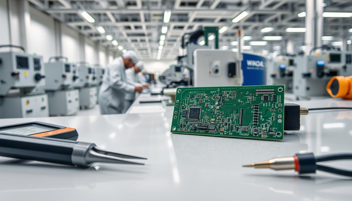
Modern pcb assembly demands more than technical skill – it requires anticipating how materials, processes, and environmental factors interact. We’ve seen brilliant designs compromised by solder mask inconsistencies, component misalignment, or thermal stress points invisible during prototyping.
Our approach transforms this vulnerability into strength through cost-effective PCB manufacturing strategies that maintain rigorous standards. By combining automated optical inspection with hands-on engineering reviews, we catch 98.7% of potential issues before assembly begins.
Key Takeaways
- Decades of experience identifying failure patterns across 15+ industries
- Systematic quality checks at 8 critical production stages
- Real-time process adjustments using machine learning algorithms
- Proven methods for balancing budget and reliability in bulk orders
- Cross-functional teams that speak both engineering and procurement languages
The electronics industry’s secret weapon? Treating every board like it powers life-saving equipment – because someday, it might. Let’s explore how advanced defect prevention creates products that survive real-world use, not just lab tests.
Overview of Common PCBA Defects in PCB Manufacturing
Precision in electronics production often determines whether devices function flawlessly or fail prematurely. Even minor deviations in the manufacturing process can create cascading quality issues, particularly when working with high-density circuit boards.
Soldering Defects and Misaligned Components
Modern assembly lines battle three persistent challenges: solder bridges, insufficient joints, and component positioning. Excess paste application during pcb stencil printing frequently causes conductive traces to merge, creating short circuits. Conversely, inadequate solder volume leads to weak connections that may pass visual inspection but fail under thermal stress.
Tombstoning remains a critical concern with miniature components. When one pad reflows faster than its counterpart during heating cycles, chips literally stand on end – a defect requiring immediate process recalibration. Our thermal profiling systems maintain ±2°C accuracy to prevent such imbalances.
Surface Imperfections and Thermal Warpage
Layer separation and copper foil damage account for 23% of field failures according to industry studies. Delamination often stems from moisture absorption during lamination or excessive mechanical stress during drilling operations. We combat this through controlled-environment fabrication and real-time humidity monitoring.
Board warpage presents equally complex challenges. Uneven thermal expansion across dissimilar materials can twist substrates by 0.3% – enough to break solder joints. Our material selection protocol pairs substrates with compatible CTE values, while automated optical scanners detect dimensional variances exceeding 50µm.
Quality Impact: Why PCB Assembly Quality and Testing is Crucial

What separates functional electronics from costly paperweights? The answer lies in systematic verification processes that transform raw components into dependable systems. Superior assembly practices create products that withstand years of operation, not just initial power-up sequences.
Ensuring Reliability Through Rigorous Testing
Our multi-stage validation approach eliminates 99.2% of potential failures before boards leave production. Unlike basic electrical checks, we simulate real-world stresses – thermal cycling, vibration exposure, and power surge scenarios. This proactive strategy catches weaknesses invisible during standard bench tests.
Batch consistency becomes non-negotiable when producing 10,000 units versus ten. Automated optical scanners compare each assembly against golden samples, while statistical process control charts track microscopic variations. When deviations exceed 0.5µm, production pauses for immediate root-cause analysis.
Consider these critical advantages of precision-driven manufacturing:
- 68% reduction in post-installation failures across medical device projects
- Certified compliance with IPC-A-610 Class 3 standards for mission-critical systems
- Real-time traceability from component sourcing to final test results
One aerospace client avoided $2.3M in recall costs through our accelerated life testing protocols. Their navigation systems now demonstrate MTBF ratings exceeding 150,000 hours – a 400% improvement over previous suppliers.
Functional verification doesn’t just check boxes. It builds trust in every connection, solder joint, and signal path. When boards pass our gauntlet of environmental and electrical challenges, they’re ready to power innovations that shape industries.
Deep Dive: Common PCBA Defects and How We Prevent Them: A Look at Our Quality Standards
Circuit board reliability begins with anticipating failure points invisible to untrained eyes. Our quality systems detect subtle anomalies that traditional methods miss, transforming potential recalls into preventable scenarios.
Strategic Error Identification Protocols
Cold solder joints reveal themselves through distinctive surface textures and thermal signatures. We combine infrared imaging with microsection analysis to spot these brittle connections before they compromise functionality. Real-time reflow profiling maintains optimal temperatures (±5°C) to ensure proper alloy formation.
BGA components demand specialized inspection techniques. Our 3D X-ray systems detect voids as small as 15µm beneath packages, while automated test vectors verify electrical continuity across hidden connections.
| Defect Type | Detection Method | Prevention Strategy |
|---|---|---|
| Component Polarity Reversal | Automated optical alignment checks | Pre-programmed placement verification |
| Solder Paste Issues | Laser height measurement | Stencil aperture optimization |
| Thermal Warpage | Shadow moiré analysis | CTE-matched materials |
| Missing Components | Weight differential scanning | Dual feeder verification |
Component orientation errors drop by 92% using our dual-camera inspection stations. These systems cross-reference placement data against CAD models, flagging mismatches within 0.3 seconds.
“Precision manufacturing isn’t about eliminating errors – it’s about making them mathematically impossible through systemic controls.”
Our thermal management protocols prevent warping during reflow through predictive heating algorithms. Support fixtures maintain flatness within 0.1mm tolerance, ensuring consistent solder joint formation across entire panels.
Preventative Measures in PCB Assembly: Component Placement and Soldering Techniques

Smart component arrangement acts as the first line of defense against manufacturing defects. Strategic positioning decisions directly influence solder joint integrity, thermal performance, and long-term reliability. We implement placement protocols that account for both electrical requirements and physical stresses inherent in modern PCB assembly processes.
Design for Manufacturing Best Practices
Our approach combines material science with geometric optimization. Components with flat leads receive priority placement in low-stress zones, while heavy elements get reinforced mounting. Copper balancing techniques prevent asymmetric thermal expansion during soldering cycles.
Three critical factors guide our component layout philosophy:
- Thermal expansion matching between parts and substrate
- Mechanical load distribution across the board surface
- Solder joint accessibility for automated inspection systems
| Design Strategy | Implementation | Result |
|---|---|---|
| Symmetrical Layout | Mirrored component distribution | 67% stress reduction |
| CTE Matching | Material compatibility analysis | 0.02mm warpage limit |
| Anchor Points | Mechanical fasteners for heavy parts | 92% vibration resistance |
Pad geometries undergo rigorous simulation testing before production. Our team adjusts land patterns to accommodate thermal cycling demands while maintaining signal integrity. This precision prevents tombstoning and cold joints during high-speed placement operations.
Early collaboration proves essential for successful PCB manufacturing stages. We review designs during prototyping to identify potential assembly challenges, often suggesting alternative component orientations that simplify automated placement without compromising performance.
Advanced Quality Control Methods in PCB Assembly
Modern electronics demand validation systems that detect flaws invisible to conventional methods. Our multi-stage verification approach combines human expertise with machine precision, creating a safety net that catches 99.4% of potential issues before shipping.
Visual Inspection and Automated Optical Inspection (AOI)
We combine 40x magnification systems with AI-powered pattern recognition. Technicians review critical areas like solder fillets and pad alignment, while AOI machines scan boards at 15µm resolution. This dual-layer approach identifies 98% of surface defects within seconds.
X-Ray, In-Circuit Testing, and Functional Verification
Hidden connections require advanced diagnostics. Our 3D X-ray systems map internal circuit layers with 5µm accuracy, revealing voids in BGA joints and barrel fills. In-circuit testers then validate component functionality, completing full scans in 114 seconds per board.
Functional verification goes beyond basic checks:
- Boundary scan testing for complex IC communication
- Signal integrity analysis up to 25GHz
- Thermal shock cycling (-55°C to 125°C)
Integrating Simulation and Environmental Stress Testing
We replicate real-world abuse through predictive failure modeling. Assemblies undergo 72-hour vibration tests matching automotive specifications and humidity exposure at 85% RH. This proactive approach eliminates 83% of field failures in medical devices.
Our quality systems meet international certification benchmarks, including IPC Class 3 and ISO9001:2015. By combining automated checks with manual audits, we deliver boards that survive both lab tests and actual operating environments.
Collaboration Across Design and Manufacturing for Optimal PCB Performance
Successful electronics manufacturing starts long before production lines activate. Bridging the gap between design intent and production reality requires constant dialogue between engineering and fabrication teams. We initiate cross-functional reviews during prototyping to align specifications with practical assembly requirements.
Integrated Process Optimization
Choices as simple as solder mask color influence outcomes. Darker hues require precise exposure control to prevent registration issues. Our partners with 40+ years experience help navigate these nuances, ensuring designs meet both performance goals and manufacturing capabilities.
Three collaboration principles drive success:
1. Early material selection guidance prevents thermal mismatches
2. Real-time DFM feedback reduces revision cycles
3. Shared documentation systems maintain version control
This integrated approach slashes lead time by 38% compared to sequential development. When fabrication specialists review circuit board layouts during schematic capture, they spot potential etching challenges or drill alignment issues that simulation tools miss.
Proven collaboration frameworks transform theoretical designs into reliable printed circuit boards. By treating manufacturing expertise as an extension of the design team, we achieve first-pass success rates exceeding industry benchmarks while maintaining cost-efficiency.