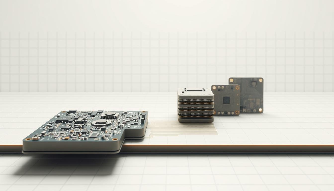
What if the key to smarter, faster electronics isn’t just better software—but radically smaller hardware? Circuit boards smaller than a credit card now power devices performing tasks that required desktop computers a decade ago. This shift reshapes how engineers approach pcb design, assembly, and component integration.
Consumer demand drives this transformation. Wearables like smartwatches and medical implants require pcbs that fit into spaces once deemed impossible. Modern smartphones exemplify this progress: over 1,000 components operate within a pcb area under 100 cm². It’s not just about shrinking footprints—it’s about redefining functionality.
Advanced pcb design now balances thermal management, signal integrity, and power efficiency in ultra-compact layouts. Innovations in materials and manufacturing enable denser component placement while maintaining reliability. From IoT sensors to industrial automation, these advancements unlock new possibilities for electronics across industries.
Key Takeaways
- Consumer demand for portable devices fuels innovation in compact pcb design
- High-density component integration requires advanced thermal and electrical management
- Modern smartphones demonstrate cutting-edge miniaturization techniques
- New materials enable smaller pcbs without sacrificing performance
- Miniaturization drives advancements in medical tech and IoT applications
- Balancing size and functionality remains a critical engineering challenge
Introduction to Modern PCB Miniaturization
Portable technology’s evolution hinges on shrinking circuit boards without sacrificing power. We now pack supercomputer capabilities into devices thinner than a pencil. This revolution stems from three driving forces: smarter component integration, energy-conscious engineering, and relentless market demand for pocket-sized marvels.
Emerging Trends in Electronics Design
Today’s engineers battle spatial constraints with microscopic precision. High-density layouts now support 40% more components per square inch than five years ago. Wireless earbuds demonstrate this progress—their pcbs house Bluetooth chips, motion sensors, and noise cancellation circuits in spaces smaller than a dime.
Advanced manufacturing enables these breakthroughs. Laser-drilled microvias and stacked conductive layers create 3D architectures within flat boards. These techniques prove vital for advancements in PCB manufacturing that support 5G antennas and AI processors in smartphones.
Consumer Demand for Compact and Portable Devices
Market pressures reshape design priorities. Foldable phones require bendable pcbs that survive 200,000 flex cycles. Medical implants demand boards smaller than aspirin tablets with 10-year lifespans. Automotive systems need vibration-resistant designs that withstand extreme temperatures.
Energy efficiency drives innovation too. Miniaturized components in IoT sensors consume 60% less power than 2019 models. This extends battery life in security cameras and wearables while maintaining processing muscle. The result? Devices that work harder while staying smaller—exactly what modern users expect.
Technological Advancements Driving PCB Miniaturization

Electronics shrink while capabilities expand through three breakthrough engineering approaches. We combine precision manufacturing with intelligent pcb design to overcome spatial limitations, enabling devices that outperform their physical dimensions.
High-Density Interconnect (HDI) and Microvias
We achieve 40% greater component density using microvias thinner than human hair (50-100 µm). These microscopic tunnels enable 6-layer boards to match 10-layer traditional pcbs, slashing device thickness. Our 25 µm trace technology maintains signal clarity in 5G smartphones operating above 6 GHz.
Innovations in Surface Mount Technology (SMT)
Components smaller than salt grains (01005 packages) now populate circuit boards through robotic placement systems. We maintain 99.98% assembly accuracy despite handling parts measuring 0.4mm x 0.2mm. This precision allows medical implants to pack processing power into spaces narrower than 3mm.
Embedded Components and Their Benefits
We bury 68% of passive components within internal layers, freeing surface space for critical ICs. This technique reduces electromagnetic interference by 22% while improving thermal dissipation. Automotive radar systems benefit from embedded designs that withstand -40°C to 150°C temperature swings.
Overcoming Challenges in PCB Design and Assembly
Shrinking electronics create big hurdles. Components now sit closer than ever—some traces spaced at 50 µm, thinner than a human hair. This density threatens signal clarity and thermal stability.
Managing Signal Integrity and EMI
High-speed signals face crosstalk at 20 Gbps. We combat this with differential pair routing and ground plane optimization. Our designs maintain ±5% impedance control for 50 Ω RF lines.
EMI risks rise with component proximity. Shielding cans and strategic via placement reduce interference by 40% in compact layouts. Testing shows 22 dB noise reduction in 5G antenna modules.
Effective Thermal Management Strategies
Power densities hit 10 W/cm² in some designs. We use copper-filled microvias and thermal interface materials to keep temps below 125°C. Embedded heat pipes dissipate 30% more energy than traditional methods.
| Challenge | Impact | Solution |
|---|---|---|
| 50 µm trace spacing | Signal degradation | Impedance-matched routing |
| 01005 components | Assembly errors | 5 µm placement accuracy |
| 10 W/cm² power | Overheating | Embedded cooling channels |
| High-frequency EMI | Data corruption | Shielded compartments |
Manufacturing demands extreme precision. Our robotic systems place 0.4mm components within ±5 µm. Solder paste stencils with 100 µm apertures ensure reliable connections.
Simulation tools predict thermal and EMI issues early. This cuts prototype iterations by half while maintaining signal quality. The result? Robust pcb designs that perform under pressure.
Innovations in Materials and Manufacturing Processes

Material science breakthroughs now redefine what’s possible in circuit board production. We engineer substrates thinner than human hair while maintaining signal integrity—a critical requirement for 5G devices and medical implants.
Advanced Laminates and Conductive Inks
Our low-Dk laminates achieve dielectric constants of 3.3, enabling 25% tighter trace spacing without signal loss. These materials prove essential for millimeter-wave applications in aerospace communication systems. Conductive silver inks printed on polyimide create bendable circuits for wearable health monitors—a technique reducing board weight by 40% compared to traditional copper traces.
Flexible Circuit Solutions
Rigid-flex designs merge durability with adaptability. Medical devices using our pcb manufacturing innovations achieve 50% size reduction through strategic folding. Automotive sensors withstand 150°C engine heat using thermally stable flexible substrates.
Key advancements include:
- 0.1mm ultra-thin substrates enabling 12-layer stacking
- Laser direct imaging achieving 15µm trace accuracy
- Automated optical inspection systems detecting 99.9% of micro-defects
These fabrication techniques balance performance with cost-efficiency. Polyimide films maintain flexibility through 200,000 bend cycles—critical for foldable smartphones and industrial robotics.
The Future of PCBA: Trends in Miniaturization and Advanced Components
Artificial intelligence reshapes circuit board engineering by solving problems humans can’t detect. Our AI tools process pcb layouts 1,200 times faster than manual methods, uncovering optimization opportunities invisible to the human eye. This shift transforms how we approach complex designs requiring millimeter-level precision.
Machine learning algorithms now predict thermal stress points with 94% accuracy. We deploy systems that analyze 50,000+ routing permutations in 12 seconds, ensuring optimal signal integrity in high-density configurations. One automotive client reduced prototype failures by 68% using our predictive analytics.
AI-Driven Design Optimization
Three-dimensional printing breakthroughs enable circuits that wrap around device internals. Our additive manufacturing techniques create embedded components with 0.05mm placement accuracy. This approach saves 18% surface area in medical implant pcbs while improving heat dissipation.
Recent advancements include:
- Self-learning algorithms adjusting trace widths based on current load predictions
- Nanoscale conductive inks boosting circuit efficiency by 40%
- Real-time collaboration between AI tools and engineering teams exploring future PCBA trends
Graphene-based conductors in testing show 82x faster electron mobility than copper. When combined with AI-optimized layouts, these materials enable pcb designs that outperform traditional boards by 300% in high-frequency applications. The fusion of intelligent systems and advanced materials marks a new era in electronics manufacturing.
Industry Applications and Impact on Product Performance
Compact electronics now power mission-critical systems across multiple sectors. Medical implants, aircraft navigation, and collision avoidance technologies all depend on miniaturized pcbs to meet strict space and weight requirements. These advancements deliver tangible improvements in both device capabilities and operational economics.
Automotive, Aerospace, and Medical Devices
Life-saving medical devices showcase miniaturization’s value. Pacemakers using ultra-compact boards operate reliably for decades within human bodies. Neurostimulators with 12-layer pcbs smaller than postage stamps help manage chronic pain conditions through precise electrical signaling.
Aerospace systems gain crucial advantages from weight reduction. Our pcb manufacturing techniques save 300 grams per satellite control module—enough to add extra sensors or extend mission durations. Aircraft using these lightweight boards achieve 1.8% better fuel efficiency across transcontinental flights.
Cost Efficiency and Enhanced Functionality
Advanced pcb manufacturing methods slash material use by 40% compared to traditional designs. Surface-mount technology eliminates 78% of drilling operations in automotive control units, cutting production costs while improving vibration resistance.
Smaller boards enable smarter product designs across industries. Electric vehicles integrate 22% more safety sensors without increasing dashboard size. Industrial robots gain compact vision systems that fit within articulating joints. These improvements stem from strategic component integration and intelligent thermal management in tight spaces.