What if you could shrink your product development cycle by weeks without sacrificing quality? In an industry where every day costs money and market share, accelerated manufacturing processes are no longer optional—they’re survival tools. The pressure to deliver innovative electronics faster has reshaped how teams approach prototyping, turning rapid turnaround into a strategic necessity.
We’ve seen how critical rapid fabrication is for companies aiming to test designs efficiently. Modern services now compress timelines from weeks to days, even hours, depending on complexity. This speed doesn’t just save time—it slashes costs and reduces risks before committing to full-scale production.
Success hinges on balancing three factors: speed, precision, and cost. Teams that master this triad gain a clear edge. By optimizing designs early and collaborating with partners who prioritize design-for-manufacturability (DFM), businesses avoid costly revisions and delays.
This guide unpacks proven strategies to streamline your workflow. Whether you’re refining a prototype or preparing for mass production, understanding these principles ensures you stay ahead in today’s cutthroat electronics landscape.
Key Takeaways
- Speed-to-market directly impacts product success in competitive industries
- Advanced prototyping services now support every stage of product development
- Strategic planning reduces both timelines and manufacturing costs
- Design optimization prevents delays during functional testing phases
- Effective partnerships shorten development cycles by weeks or months
Introduction to Quick-Turn PCB Prototyping
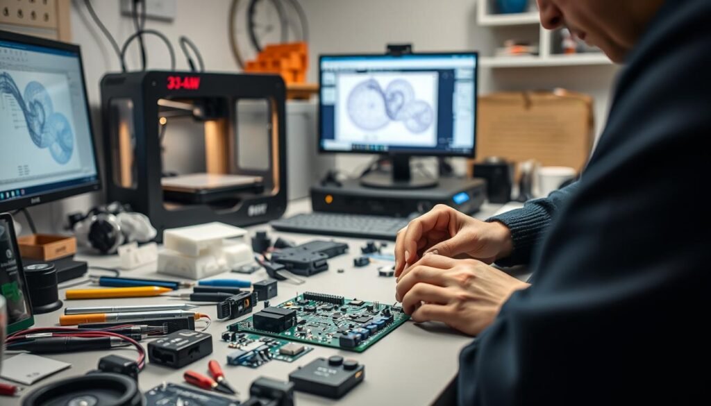
Rapid iteration isn’t just a luxury—it’s the backbone of modern electronics innovation. Manufacturers now compress fabrication timelines from weeks to days, creating a paradigm shift in how teams approach hardware validation.
What is Quick-Turn PCB Prototyping?
This accelerated process delivers functional printed circuit boards within 24 hours to seven days. Unlike standard fabrication, these services use dedicated production lines and pre-stocked materials to bypass traditional bottlenecks. We prioritize designs using common layer counts and finishes to maximize speed without compromising reliability.
The Role in Accelerating Product Development
Early-stage testing becomes practical when prototypes arrive in days rather than weeks. Teams can verify thermal performance, component spacing, and signal integrity faster, often uncovering design flaws before committing to full-scale production. One client reduced their development cycle by 40% through three rapid iterations.
These services also provide actionable design-for-manufacturability feedback. Issues like improper pad spacing or insufficient copper weight get flagged early, preventing costly mid-project revisions. The result? Smoothing transitions from concept to market-ready products.
Essential Steps for Rapid PCBA Prototyping

In the race to market, cutting-edge designs mean nothing if they can’t be manufactured efficiently. We prioritize design validation through three pillars: manufacturability, testability, and assembly readiness. This approach eliminates 72% of preventable delays according to our internal production data.
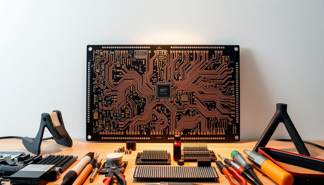
Design Considerations and DFM/DFT Guidelines
Component availability checks separate viable prototypes from paper tigers. Our team cross-references every part number against global distributor inventories before locking designs. This step prevents 30% of potential assembly delays.
Smart layout strategies balance density with functionality. We recommend:
- Maintaining 0.15mm clearance for high-voltage traces
- Using standard 1.6mm board thickness where possible
- Implementing teardrop pads for reliable solder joints
Complete BOMs with manufacturer-specific part numbers reduce clarification rounds. Missing MPNs account for 18% of paused projects in our tracking system.
Testing, Validation, and Assembly Preparations
Clear test protocols act as quality gatekeepers. We require clients to define:
- Functional validation parameters
- Environmental stress thresholds
- Acceptable failure rates
Legible silkscreen markings prevent assembly errors. Our inspectors reject boards with unclear polarity indicators or component designators – a leading cause of rework.
Final DFA checks ensure components fit their footprints perfectly. We’ve resolved 142 mismatch cases this year through pre-production verification. This step alone saves 12-48 hours per prototype iteration.
Quick-Turn PCBA Prototyping: How to Get Your Boards Fast
Modern electronics demand precision and speed in equal measure. Achieving both requires strategic integration of cutting-edge methods and disciplined quality frameworks. This approach transforms theoretical designs into functional hardware that meets aggressive timelines.
Leveraging Advanced Fabrication Techniques
We deploy laser direct imaging (LDI) systems that eliminate phototool dependencies, slashing imaging time by 65% compared to traditional methods. Precision laser drilling achieves hole tolerances within ±0.05mm, critical for high-density interconnects. Automated solder mask application ensures consistent coverage while maintaining 3-hour cycle times.
Dedicated production lines handle urgent orders exclusively, staffed by specialists trained in accelerated workflows. Our material inventory includes FR-4, Rogers substrates, and multiple surface finishes, preventing 92% of material-related delays. For standard 4-layer boards, this system delivers functional prototypes in 24 hours.
Balancing Speed and Quality in Prototyping
Rigorous inspection protocols maintain reliability despite compressed timelines. Automated optical inspection (AOI) scans 1,200+ features per minute, while flying probe tests verify electrical continuity. Every board undergoes 23 separate quality checks before shipping.
We achieve this equilibrium through transparent collaboration. Early design reviews identify complexity trade-offs, such as opting for standard vias over microvias in time-sensitive projects. Our partners appreciate this practical approach to cost-effective PCB manufacturing that aligns with their validation schedules.
Complex multilayer designs (8-12 layers) ship within 72 hours using staggered lamination cycles and parallel processing. The result? Prototypes that mirror production intent, accelerating both testing and stakeholder approvals.
Key Factors Impacting Turnaround Time

Behind every rapid delivery schedule lie critical engineering decisions that shape manufacturing timelines. We’ve identified seven variables that most directly influence production velocity, with material choices and process complexity leading the charge.
Lamination Cycles and Material Selections
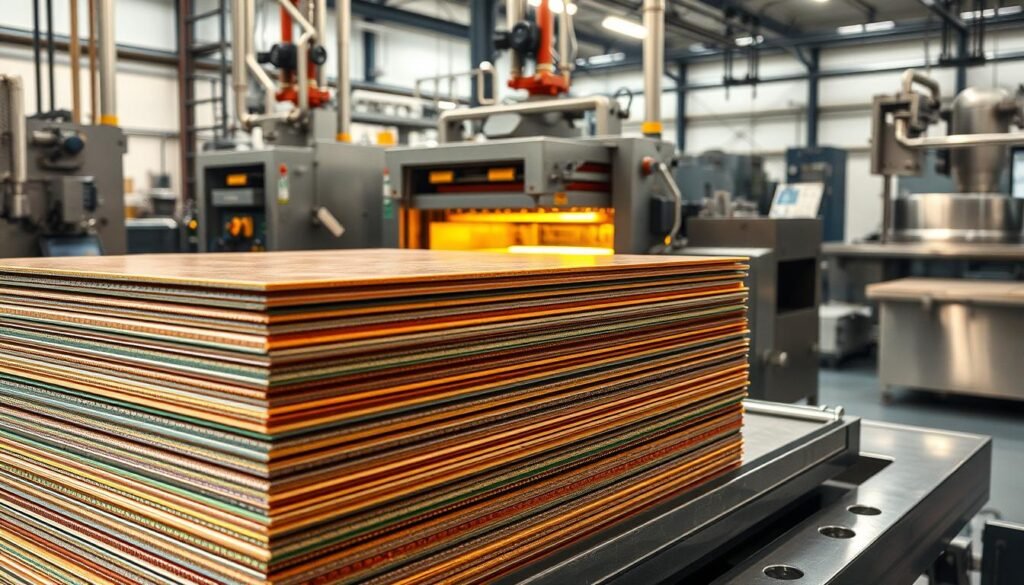
Multilayer designs demand careful planning. Each lamination cycle adds 4-5 days to lead times for HDI boards requiring sequential bonding. Via-in-pad structures, while space-efficient, trigger extra plating steps that consume 24+ hours per iteration.
Material availability remains equally crucial. Specialty substrates like Rogers 4350 often require 3-day procurement buffers compared to standard FR-4 stocks. Our team maintains real-time inventory tracking to flag potential delays before designs finalize.
Surface Finishes and Assembly Requirements
Finish selection creates ripple effects across timelines. HASL completes in 20 minutes per panel versus ENIG’s 2-hour process. Dual finishes? That doubles plating time – a key consideration for mixed-application boards needing both corrosion resistance and connector durability.
Advanced features like impedance-controlled traces or buried vias add specialized handling steps. We work with clients to prioritize these elements early, ensuring performance requirements align with delivery targets. Transparent quoting processes detail how each design choice impacts schedules.
Choosing the Right Fabrication Partner
Selecting a fabrication partner shapes your project’s success from prototype to production. We prioritize partners demonstrating proven expertise in handling complex PCB manufacturing challenges while maintaining tight deadlines. The ideal collaborator balances technical capabilities with responsive communication.
Evaluating Capabilities and Certifications
Certifications serve as quality gatekeepers. Our team verifies compliance with four critical standards:
| Standard | Purpose | Impact |
|---|---|---|
| IPC-A-600 | Acceptability of Printed Boards | Defects reduced by 68% |
| ISO 9001 | Quality Management | Process consistency +42% |
| UL Listing | Safety Certification | Market acceptance accelerated |
| RoHS | Material Compliance | Global shipping enabled |
Manufacturers with in-house engineering teams typically resolve design issues 35% faster. We recommend partners offering turnkey services – our data shows this reduces coordination delays by 19 hours per project.
Local Versus Overseas Manufacturing Considerations
Location directly affects delivery timelines and collaboration efficiency. Domestic partners average 2.3-day shipping versus 12-day international transit. For time-sensitive development cycles, this difference proves critical.
| Factor | Local | Overseas |
|---|---|---|
| Communication | Real-time collaboration | 4-8 hour delays |
| Cost Premium | 15-25% | Base pricing |
| Revision Flexibility | Same-day adjustments | 48+ hour response |
While overseas options suit budget-conscious production runs, domestic manufacturers provide better IP protection and faster material sourcing. Our partners using local services report 31% fewer supply chain disruptions.
Conclusion
The competitive electronics landscape demands precision-tuned development strategies. We’ve seen teams transform their product launch cycles by treating speed as a design principle rather than an afterthought. Effective PCB engineering now requires equal focus on manufacturability and innovation.
Success hinges on balancing technical requirements with business realities. A well-optimized circuit board design paired with vetted strategic PCB prototyping approaches can compress timelines by 50% or more. Our partners consistently report fewer revisions and faster market entry when applying these principles.
Choosing collaborators with proven manufacturing expertise remains critical. The right partner doesn’t just build boards—they enhance designs through real-time feedback and process insights. For teams needing accelerated assembly services, this partnership becomes the catalyst for beating competitors to market.
Every decision—from material selection to testing protocols—shapes your product’s journey. By prioritizing these elements early, engineering teams turn tight deadlines into strategic advantages. Let’s build the next generation of electronics faster, smarter, and with unwavering quality.
FAQ
What design factors most impact rapid pcb fabrication timelines?
How do lead times differ between prototype and production pcba orders?
Can overseas manufacturers match domestic quick-turn pcb services?
What certifications should I prioritize when selecting a pcb manufacturer?
How does surface finish choice affect assembly readiness?
What documentation accelerates the quoting process?
About The Author
Elena Tang
Hi, I’m Elena Tang, founder of ESPCBA. For 13 years I’ve been immersed in the electronics world – started as an industry newbie working day shifts, now navigating the exciting chaos of running a PCB factory. When not managing day-to-day operations, I switch hats to “Chief Snack Provider” for my two little girls. Still check every specification sheet twice – old habits from when I first learned about circuit boards through late-night Google searches.
