When working with PCBA manufacturers, you’ll inevitably encounter a DFM Report—a critical document that can make or break your project’s success. Understanding how to read and interpret these reports effectively can save you time, money, and countless headaches during production. This comprehensive guide will walk you through the essential components of a DFM Report, how to interpret common issues, and how to implement the feedback to improve your designs.
What Is a DFM Report and Why Is It Important?
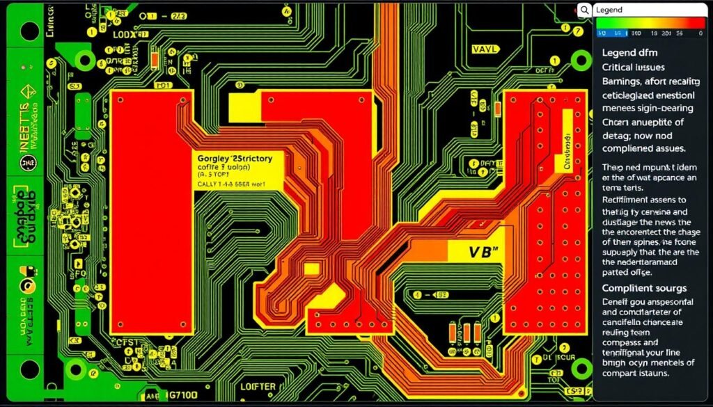
A typical DFM Report highlights potential manufacturing issues before production begins
A Design for Manufacturing (DFM) Report is a detailed evaluation document created by PCBA factories to assess whether your PCB design can be manufactured efficiently and reliably. Think of it as a pre-flight check that identifies potential issues before your design goes into production.
The primary purpose of a DFM Report is to bridge the gap between design intent and manufacturing reality. While your design might work perfectly in simulation, real-world manufacturing constraints can introduce unexpected challenges that affect functionality, reliability, and cost.
Key Benefits of Understanding Your DFM Report
- Reduced manufacturing defects and field failures
- Lower production costs by addressing issues early
- Faster time-to-market by minimizing design revisions
- Improved relationship with your manufacturer through clearer communication
- Enhanced product quality and reliability
According to industry data, addressing DFM issues early in the design process can reduce manufacturing costs by up to 50% and cut development time by 30%. These numbers highlight why understanding your DFM Report is not just helpful—it’s essential for competitive product development.
The Anatomy of a PCBA DFM Report
While DFM Reports can vary between manufacturers, most follow a similar structure with key sections that address specific aspects of your design. Understanding this structure helps you navigate the report efficiently and focus on the most critical issues.
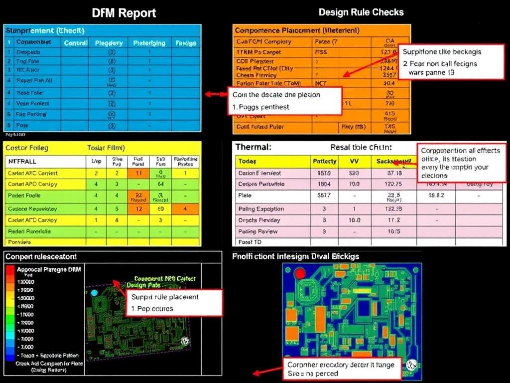
A typical DFM Report contains several key sections addressing different aspects of manufacturability
1. Design Rule Checks (DRC)
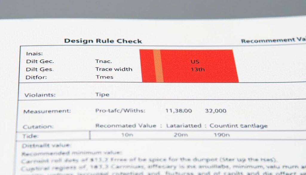
This section evaluates whether your design meets the manufacturer’s minimum requirements for trace widths, spacing, hole sizes, and other physical parameters. It typically includes:
- Trace width and spacing violations
- Minimum drill size and annular ring issues
- Clearance violations (component-to-component, component-to-board edge)
- Copper balance and plane issues
2. Component Placement Analysis
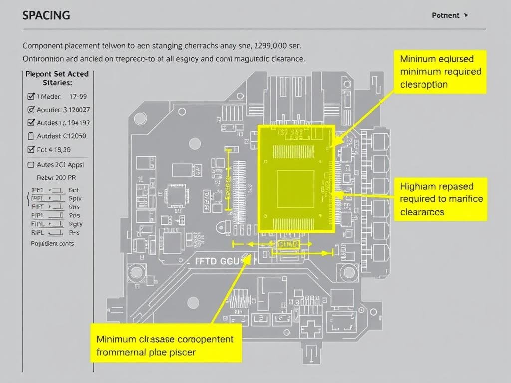
This section evaluates the placement of components on your PCB and identifies potential assembly issues:
- Component spacing for pick-and-place machines
- Orientation and polarity of components
- Accessibility for automated and manual assembly
- Component proximity to board edges and mechanical features
3. Material and Process Compatibility
This section assesses whether your specified materials and processes are compatible with the manufacturer’s capabilities:
- PCB substrate material availability and compatibility
- Surface finish compatibility with assembly processes
- Special requirements (impedance control, high-frequency materials)
- RoHS and other regulatory compliance issues
4. Thermal and Signal Integrity Analysis
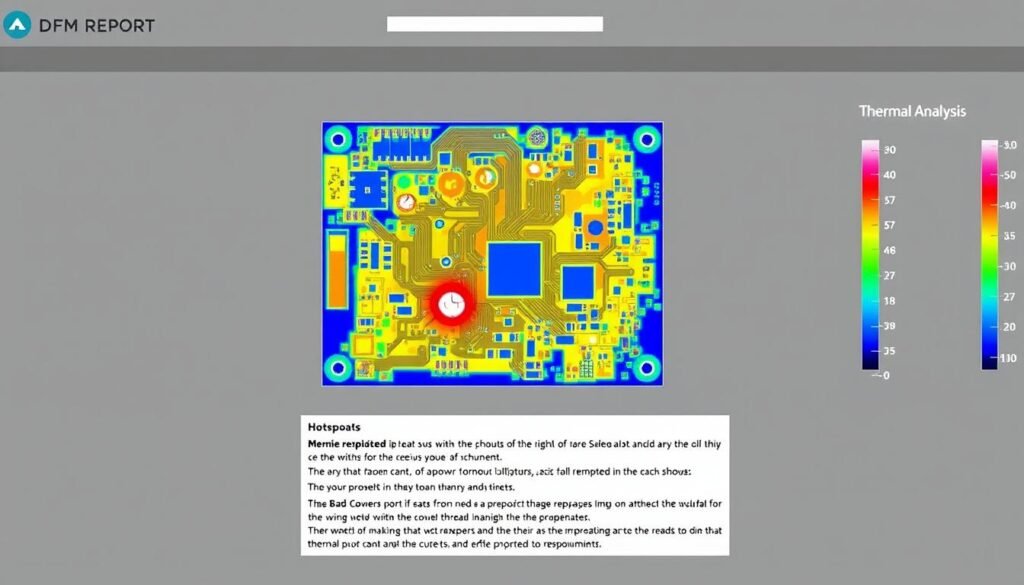
More advanced DFM Reports may include analysis of thermal management and signal integrity:
- Heat dissipation concerns for high-power components
- Signal integrity issues for high-speed traces
- Power distribution network analysis
- EMI/EMC considerations
5. Recommendations and Action Items
The final section typically provides specific recommendations to address identified issues:
- Prioritized list of required changes
- Optional improvements for yield and reliability
- Alternative solutions for critical issues
- Cost implications of different options
How to Read DFM Report Data Formats
DFM Reports present information in various formats, from tables and diagrams to color-coded visualizations. Understanding these formats is key to extracting actionable insights.
Tabular Data in DFM Reports
| Issue Type | Location | Current Value | Required Value | Severity |
| Trace Width | Top Layer, Net: SIGNAL_3 | 0.15mm | 0.20mm | High |
| Annular Ring | Via at X:45.2, Y:78.3 | 0.05mm | 0.075mm | Medium |
| Component Clearance | C12 to R45 | 0.5mm | 0.8mm | Low |
Tables like this example typically list specific issues, their locations, current values, required values, and severity levels. Focus first on high-severity issues, as these are most likely to cause manufacturing failures.
Color-Coded Visualizations
Many DFM Reports include color-coded visualizations of your PCB to highlight issues:
- Red: Critical issues that must be fixed
- Yellow: Warnings that may affect yield or reliability
- Green: Areas that meet all manufacturing requirements
- Blue: Informational highlights or suggestions
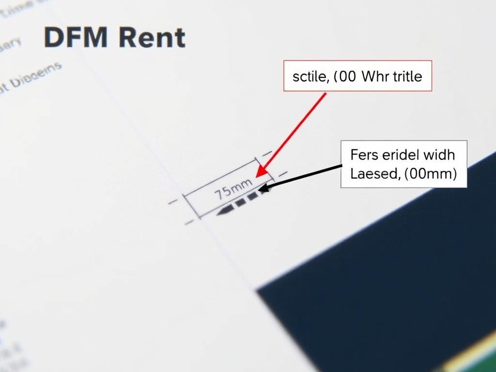
Measurement Annotations
Look for specific measurements and annotations that highlight exactly where and how your design deviates from manufacturing requirements:
Interpreting Common DFM Report Issues
Certain issues appear frequently in DFM Reports. Understanding these common problems and how to address them will streamline your design revision process.
1. Trace Width and Spacing Violations
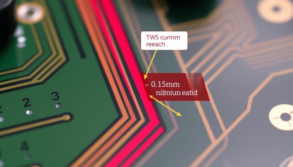
Example Issue: “Trace width of 0.15mm does not meet factory’s 0.2mm minimum for 2oz copper.”
Interpretation: The current trace is too narrow for reliable manufacturing with the specified copper weight. This could lead to broken traces during etching or current-carrying capacity issues.
Solution Options:
- Increase trace width to at least 0.2mm
- Reduce copper weight to 1oz if current-carrying capacity allows
- Re-route the trace to allow for wider paths
2. Insufficient Annular Rings

Example Issue: “Via at coordinates X:45.2, Y:78.3 has annular ring of 0.05mm, below minimum 0.075mm requirement.”
Interpretation: The copper pad surrounding the via hole is too small. During drilling, this could lead to “breakout” where the drill bit exits the copper entirely, causing an open circuit.
Solution Options:
- Increase pad size to ensure minimum annular ring requirements
- Adjust drill size smaller if possible
- Reposition the via if space constraints are an issue
3. Solder Mask Clearance Violations

Example Issue: “Solder mask clearance around BGA pads is 0.05mm, below minimum 0.075mm requirement.”
Interpretation: The gap between the solder mask and the pad is too small. This could cause the solder mask to partially cover the pad, leading to poor solder joints or assembly defects.
Solution Options:
- Increase solder mask clearance in your design software
- Consider solder mask defined (SMD) pads if appropriate for the component
- Verify that your design software’s solder mask expansion settings match manufacturer capabilities
4. Component Placement Issues

Example Issue: “Components C12 and R45 have clearance of 0.5mm, below minimum 0.8mm required for pick-and-place equipment.”
Interpretation: The components are placed too close together for the manufacturer’s assembly equipment to reliably place them without risk of collision or displacement.
Solution Options:
- Increase spacing between components to meet minimum requirements
- Consider using smaller component packages if space is constrained
- Reorient components to maximize available space
5. Thermal Relief Issues

Example Issue: “Through-hole pad P5 lacks adequate thermal relief connections to ground plane.”
Interpretation: Without proper thermal relief (the spoke-like connections between a pad and a plane), the pad will be difficult to solder because the plane acts as a heat sink.
Solution Options:
- Add thermal relief connections in your design software
- Adjust thermal relief spoke width and quantity
- For critical grounds where thermal relief isn’t desirable, note this as an exception to the manufacturer
Case Study: Implementing DFM Report Feedback
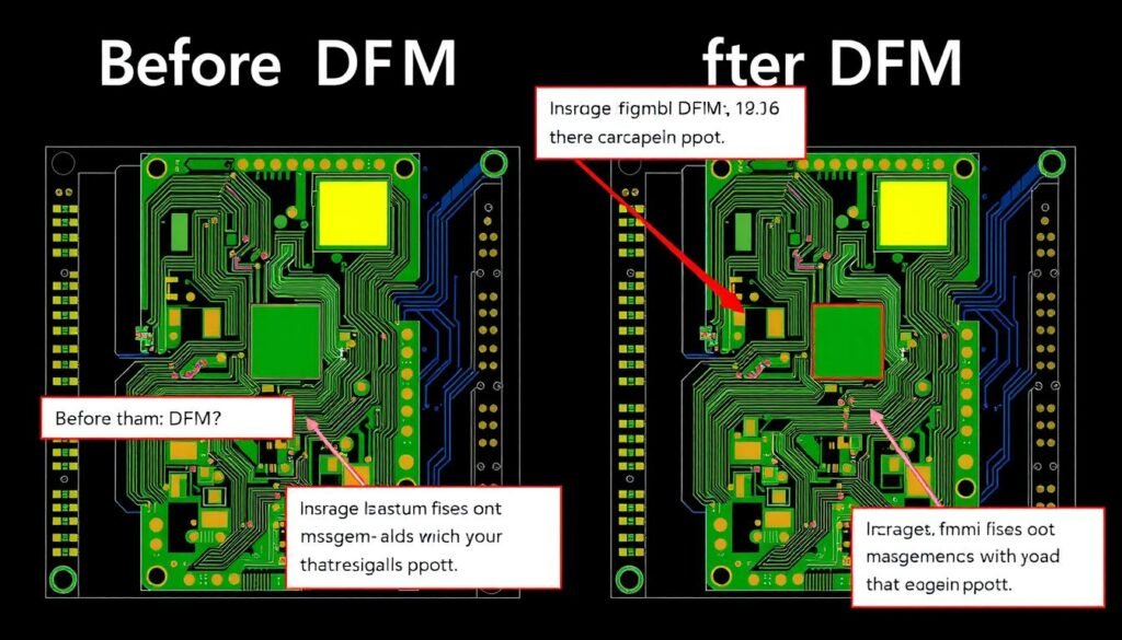
The following case study demonstrates how effectively implementing DFM feedback can transform a problematic design into a manufacturing-ready product.
Project Background
A medical device startup was developing a wearable health monitor with strict size constraints and reliability requirements. Their initial PCB design was submitted to a contract manufacturer who provided a comprehensive DFM Report.
Key Issues Identified in the DFM Report
- Multiple trace width violations (0.1mm vs. required 0.15mm minimum)
- Insufficient annular rings on 12 critical vias
- Component clearance issues around the BGA processor
- Thermal management concerns for power regulation components
- Signal integrity issues on high-speed memory interface
Implementation Process
The engineering team prioritized the issues based on severity and implemented changes in two revision cycles:
Revision 1: Critical Manufacturing Issues
- Increased all trace widths to meet minimum requirements
- Enlarged via pads to ensure proper annular rings
- Adjusted component placement to meet assembly requirements
Revision 2: Performance and Reliability Optimization
- Added copper pour areas for improved thermal management
- Implemented controlled impedance for high-speed signals
- Optimized ground plane connections for better EMI performance
Results
Before DFM Implementation
- First prototype yield: 65%
- Assembly defects: 8.5 per board
- Production cost: $42 per unit
- Development time: Extended by 6 weeks
After DFM Implementation
- Production yield: 98.5%
- Assembly defects: 0.3 per board
- Production cost: $28 per unit
- Time-to-market: Accelerated by 4 weeks
By thoroughly implementing the recommendations from the DFM Report, the company achieved a 33% reduction in production costs and significantly improved product reliability. The investment in addressing DFM issues early paid off with faster time-to-market and higher customer satisfaction.
Best Practices for Working with DFM Reports

Establish Clear Communication with Your Manufacturer
- Request the manufacturer’s design guidelines before starting your design
- Ask for clarification on any DFM issues you don’t fully understand
- Discuss trade-offs between different solution approaches
- Document all decisions and changes for future reference
Prioritize DFM Issues Effectively
Not all issues in a DFM Report are equally critical. Use this framework to prioritize your response:
| Priority | Issue Type | Impact | Response Timeframe |
| Critical | Manufacturing showstoppers (e.g., unmanufacturable features) | Production impossible | Immediate |
| High | Yield or reliability risks (e.g., marginal annular rings) | High defect rates, field failures | Before production |
| Medium | Cost or efficiency issues (e.g., panel utilization) | Higher costs, longer lead times | If budget/schedule allows |
| Low | Optimization suggestions (e.g., alternative component placement) | Minor improvements | Future revisions |
Integrate DFM Thinking Earlier in Your Design Process
- Create a DFM checklist based on previous reports
- Run internal DFM checks before submitting to manufacturers
- Consider DFM requirements when selecting components
- Document manufacturing constraints in your design requirements
Track DFM Issues Across Projects
Create a knowledge base of common DFM issues and solutions to improve future designs:
- Document recurring issues specific to your products
- Note manufacturer-specific requirements and preferences
- Share lessons learned with your design team
- Update design templates and libraries to incorporate DFM best practices
Conclusion: Turning DFM Reports into Competitive Advantage
A DFM Report is more than just a list of issues to fix—it’s a valuable tool that can help you create better products faster and at lower cost. By understanding how to read and interpret these reports effectively, you can:
- Reduce development cycles by addressing manufacturing issues early
- Lower production costs through optimized designs
- Improve product quality and reliability
- Build stronger relationships with your manufacturing partners
- Continuously improve your design capabilities
Remember that DFM is an iterative process. Each report provides insights that can be applied to future designs, creating a virtuous cycle of improvement. By embracing DFM feedback as a learning opportunity rather than a critique, you’ll develop more manufacturable designs from the start.
The most successful hardware teams don’t just react to DFM Reports—they anticipate manufacturing requirements and incorporate them into their design process from day one. With the knowledge and strategies outlined in this guide, you’re well-equipped to join their ranks and turn DFM insights into a competitive advantage for your products.
Master DFM Report Analysis
Download our free DFM Report Checklist to ensure you never miss critical manufacturing issues.
Solve DFM Issues Faster
Access our comprehensive DFM Issue Resolution Guide with step-by-step solutions for common manufacturing problems.
Expert DFM Review
Get a professional review of your PCB design before production. Our experts will identify potential manufacturing issues and provide actionable recommendations.
About The Author
Elena Tang
Hi, I’m Elena Tang, founder of ESPCBA. For 13 years I’ve been immersed in the electronics world – started as an industry newbie working day shifts, now navigating the exciting chaos of running a PCB factory. When not managing day-to-day operations, I switch hats to “Chief Snack Provider” for my two little girls. Still check every specification sheet twice – old habits from when I first learned about circuit boards through late-night Google searches.
