Impedance control has become a critical aspect of modern PCB design and manufacturing, especially as signal speeds continue to increase. When signals travel through PCB transmission lines at high frequencies, maintaining consistent impedance throughout the signal path becomes essential for preserving signal integrity. This comprehensive guide explores the fundamentals of controlled impedance, why it matters, and how engineers can implement effective impedance control strategies in their PCB designs.
What is Impedance Control in PCB Manufacturing?
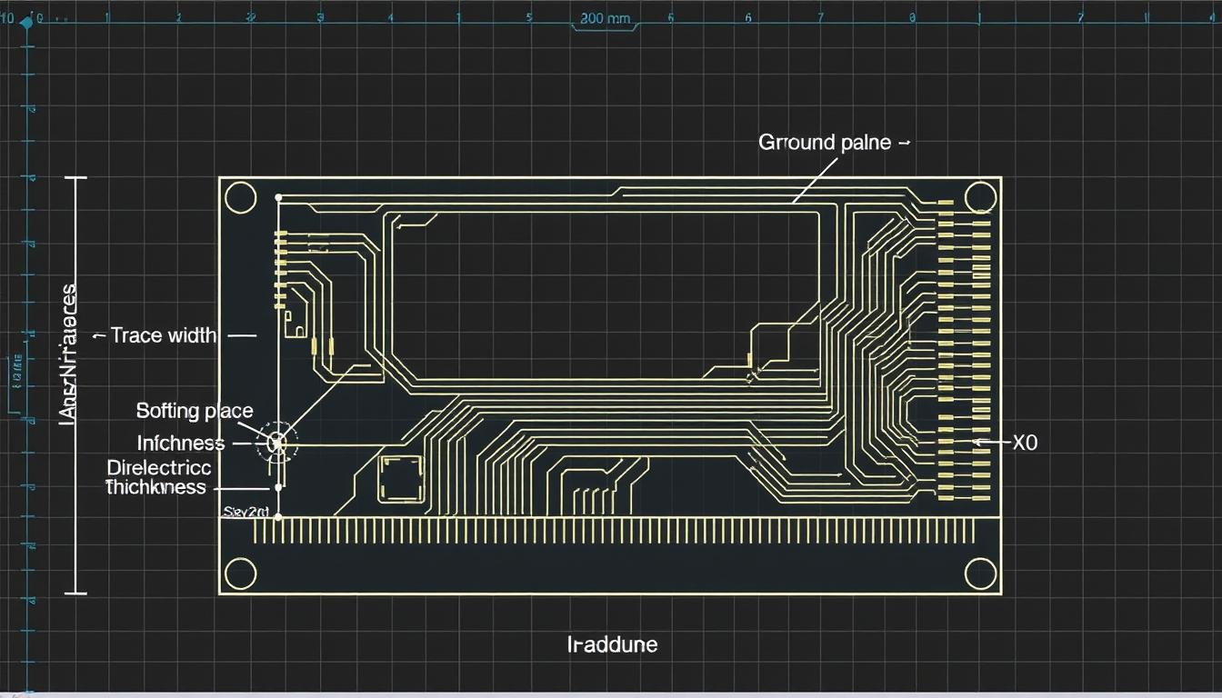
Controlled impedance refers to the characteristic impedance of transmission lines formed by PCB traces and their associated reference planes. It represents the resistance that a signal trace exerts on a signal as it propagates through the PCB. In high-frequency applications, PCB traces behave like transmission lines rather than simple conductors.
Figure 1: Cross-section of controlled impedance traces showing key parameters
Impedance is measured in Ohms (Ω) and is determined by several physical factors:
- Trace width and thickness
- Dielectric material properties (especially dielectric constant)
- Distance between the trace and reference plane
- Trace geometry and surrounding structures
When impedance varies along a transmission line, signal reflections occur. These reflections can cause signal distortion, timing errors, and other signal integrity issues that compromise the performance of high-speed circuits.
Common Types of Controlled Impedance Structures
PCB transmission lines that require controlled impedance typically fall into several categories:
- Single-ended microstrip – Trace on outer layer with reference plane beneath
- Single-ended stripline – Trace on inner layer between two reference planes
- Embedded microstrip – Similar to microstrip but with a thin dielectric covering
- Differential pair microstrip – Two coupled traces on outer layer
- Differential pair stripline – Two coupled traces on inner layer
- Co-planar waveguide – Trace with adjacent ground planes on same layer

Figure 2: Common controlled impedance structures in PCB design
Controlled Impedance Design Guide
6 Chapters – 56 Pages – 60 Minute Read
- Understanding why controlled impedance is necessary
- Stack-up design guidelines for different applications
- Step-by-step impedance calculation methods
- Common design mistakes and how to avoid them
Why Impedance Control Matters in High-Speed PCBs
As signal frequencies increase beyond 100MHz, controlling impedance becomes increasingly critical. Here’s why impedance control matters for modern PCB designs:

Figure 3: Signal reflection caused by impedance mismatch
Signal Integrity Benefits
When impedance is properly controlled throughout a transmission path:
- Minimized signal reflections – Uniform impedance reduces signal bouncing
- Reduced timing errors – Consistent propagation delay improves timing
- Better signal quality – Less distortion in digital and analog signals
- Improved rise/fall times – Cleaner transitions between logic states
Applications that typically require controlled impedance include:
- High-speed digital interfaces (DDR, HDMI, PCIe)
- RF and microwave circuits
- Telecommunications equipment
- High-performance computing
- Signal processing systems
- High-quality analog video
EMI Reduction
Properly controlled impedance also helps reduce electromagnetic interference (EMI) by:
- Minimizing radiation from signal traces
- Reducing ground bounce and power supply noise
- Improving immunity to external interference
- Helping meet regulatory compliance requirements
Calculating and Controlling Impedance
Impedance control begins with accurate calculation of trace parameters. While complex field-solving software provides the most accurate results, several approximation formulas can be used for initial design.
Single-Ended Microstrip Impedance Formula

Figure 4: Microstrip impedance calculation parameters
For a microstrip transmission line, the characteristic impedance can be approximated by:
Where:
- Z₀ = Characteristic impedance in ohms
- εᵣ = Dielectric constant of the substrate
- H = Height of dielectric between trace and ground plane
- W = Width of the trace
- T = Thickness of the trace
Differential Pair Impedance
For differential pairs, both the odd-mode impedance (Z₀) and differential impedance (Zdiff) must be considered:
The spacing between traces in a differential pair affects coupling, which influences impedance. Tighter coupling (closer spacing) reduces differential impedance.
PCB Impedance Calculator Tool
Our 2D field solver provides accurate impedance calculations for various transmission line structures.
- Calculate trace width for target impedance
- Determine impedance for existing trace dimensions
- Support for microstrip, stripline, and differential pairs
- Includes capacitance, inductance, and propagation delay calculations
Material Selection for Controlled Impedance
The dielectric materials used in PCB construction significantly impact impedance control. Key material properties to consider include:

Figure 5: Comparison of PCB materials for controlled impedance applications
Dielectric Constant (Dk/εᵣ)
The dielectric constant (Dk) of a material affects signal propagation speed and impedance. Materials with:
- Lower Dk – Faster signal propagation, higher impedance for same trace geometry
- Higher Dk – Slower signal propagation, lower impedance for same trace geometry
- Stable Dk – Consistent performance across frequency and temperature ranges
Standard FR-4 materials typically have Dk values between 3.8-4.5, while high-performance materials like Rogers or Isola can have more tightly controlled Dk values around 3.0-3.5.
Dissipation Factor (Df)
The dissipation factor (Df) measures dielectric loss. Materials with lower Df values experience less signal attenuation, which is critical for high-frequency applications.
| Material Type | Typical Dk Range | Typical Df Range | Suitable Frequency | Relative Cost |
| Standard FR-4 | 4.0-4.5 | 0.020-0.025 | Up to 1-2 GHz | Low |
| High-Speed FR-4 | 3.6-4.0 | 0.008-0.015 | Up to 5 GHz | Medium |
| Isola IS410/FR408HR | 3.5-3.7 | 0.008-0.010 | Up to 10 GHz | Medium-High |
| Megtron 6 | 3.3-3.4 | 0.004 | Up to 20 GHz | High |
| Rogers RO4350B | 3.48 | 0.0037 | Up to 30 GHz | Very High |
Material Consistency
Variation in material properties affects impedance consistency. Consider these factors:
- Resin content percentage – Higher resin content typically means lower Dk
- Glass weave style – Different weave patterns affect Dk uniformity
- Moisture absorption – Can change Dk during manufacturing and operation
- Temperature stability – Dk changes with temperature in some materials
PCB Stack-up Design for Impedance Control
The PCB stack-up design is crucial for achieving consistent impedance control. A well-designed stack-up considers signal layer placement, reference planes, and dielectric thicknesses.

Figure 6: Example of an 8-layer PCB stack-up with controlled impedance layers
Key Stack-up Considerations
Reference Planes:
- Every signal layer should have an adjacent reference plane
- Maintain consistent dielectric spacing to reference planes
- Avoid split planes under high-speed traces
- Use ground planes preferentially over power planes
Material Selection:
- Use consistent materials throughout the stack-up
- Limit prepreg types to 2-3 different styles
- Avoid prepregs with very low resin content
- Consider using core material for critical layers
Core vs. Prepreg Considerations
Understanding the difference between core and prepreg materials is essential for stack-up design:
- Core – Fully cured material with copper on both sides; thickness remains stable during lamination
- Prepreg – Semi-cured bonding material; final thickness depends on copper percentage, copper height, and prepreg type
For critical impedance control, some designers prefer core construction for outer layers to minimize thickness variation after lamination.
PCB Stack-up Design Templates
Download our pre-engineered stack-up templates for common controlled impedance applications.
- 4, 6, 8, 10, and 12-layer designs
- Optimized for different impedance requirements
- Compatible with major PCB manufacturers
- Includes material specifications and layer assignments
Trace Routing Guidelines for Controlled Impedance
Proper trace routing is essential for maintaining consistent impedance throughout the signal path. Follow these guidelines to ensure optimal performance:

Figure 7: Differential pair routing techniques for controlled impedance
Single-Ended Trace Guidelines
- Maintain consistent trace width throughout the entire path
- Keep trace width ≤ 2× the dielectric height for best impedance control
- Maintain at least 3× trace width (3W) spacing between adjacent traces to minimize crosstalk
- Avoid 90° bends; use 45° or curved traces instead
- Provide continuous reference planes beneath traces
Differential Pair Guidelines
Routing Techniques:
- Route pairs with consistent spacing throughout
- Keep spacing between traces ≤ 2× trace width
- Maintain symmetry in routing patterns
- Avoid placing components or vias between pairs
- Maintain at least 5W spacing between adjacent differential pairs
Length Matching:
- Match lengths within each differential pair to minimize skew
- Use serpentine traces for length matching
- Place serpentines near the source of mismatch
- Design serpentines with proper geometry to minimize impedance discontinuity
- Match each segment individually when changing layers
Via Considerations
Vias create impedance discontinuities that can affect signal integrity. Minimize their impact by:
- Minimizing the number of layer transitions
- Using smaller vias for high-speed signals
- Adding stitching vias near signal vias to provide return path continuity
- Placing stitching capacitors when signals change reference planes
- Staggering vias to avoid creating large voids in reference planes

Figure 8: Stitching via placement for maintaining signal return paths
Manufacturing Challenges in Impedance Control
Even with perfect design, manufacturing variations can affect impedance control. Understanding these challenges helps engineers design more robust PCBs.

Figure 9: Manufacturing tolerance effects on trace impedance
Common Manufacturing Variations
Copper Processing:
- Etching variations affecting trace width (±0.5-1.0 mil typical)
- Plating thickness variations (±0.1-0.2 mil typical)
- Trapezoidal trace profiles instead of rectangular
- Surface roughness affecting effective trace dimensions
Dielectric Processing:
- Variation in prepreg thickness after lamination
- Resin content percentage variations
- Dielectric constant variations between material batches
- Moisture absorption during processing
Impedance Tolerance Specifications
When specifying controlled impedance to manufacturers, consider these tolerance levels:
- Standard tolerance: ±10% (most economical, suitable for many applications)
- Tighter tolerance: ±5% (requires special processing, higher cost)
- Ultra-precise: ±3% (extremely challenging, significant cost premium)
Specify only the tolerance needed for your application, as tighter tolerances increase manufacturing complexity and cost.
Testing and Verification Methods
Verifying that manufactured PCBs meet impedance specifications requires proper testing methods. The most common approach uses Time Domain Reflectometry (TDR).

Figure 10: TDR impedance measurement setup with test coupon
Test Coupon Design
Test coupons are specialized PCB sections manufactured alongside the actual boards for impedance testing:
- Manufactured on the same panel as production boards
- Contains traces with same dimensions as controlled impedance traces
- Includes traces for each impedance type and layer
- Designed with proper launch points for TDR probes
- Often includes other test features (e.g., layer registration)
Time Domain Reflectometry (TDR)
TDR testing works by sending a fast-rising pulse down a transmission line and analyzing reflections:
- Measures impedance variations along the entire trace length
- Identifies specific locations of impedance discontinuities
- Provides impedance profile vs. distance
- Can measure both single-ended and differential impedance

Figure 11: TDR measurement results showing impedance profile along a trace
Cross-Section Analysis
When impedance measurements don’t match expectations, cross-section analysis helps identify the cause:
- Physically measures trace width, thickness, and dielectric height
- Evaluates trace profile (trapezoidal vs. rectangular)
- Verifies layer registration and alignment
- Identifies manufacturing issues affecting impedance
Best Practices for Impedance Control
Based on industry experience, these best practices help ensure successful impedance control in PCB manufacturing:

Figure 12: Impedance control design workflow
Design Documentation
Clearly document impedance requirements in fabrication drawings:
- Create an impedance table specifying values, tolerances, and layers
- Identify controlled impedance traces with unique widths
- Specify whether controlled impedance or controlled dielectric is required
- Include test coupon requirements
Design for Manufacturability
- Design with manufacturing tolerances in mind
- Use wider traces where possible (easier to manufacture consistently)
- Limit the number of different impedance values
- Consult with your PCB manufacturer early in the design process
- Request preliminary stack-up designs before finalizing layout
Common Mistakes to Avoid
Recommended Practices
- Use consistent trace widths for each impedance value
- Maintain continuous reference planes
- Route high-speed signals on inner layers when possible
- Add stitching vias near signal transitions
- Match differential pair lengths closely
Practices to Avoid
- Routing over split planes or plane cutouts
- Using more than three prepreg types in a stack-up
- Placing components between differential pairs
- Changing reference planes without stitching
- Assuming all FR-4 materials have identical properties
Expert PCB Design Consultation
Get personalized advice on your controlled impedance design challenges.
- Stack-up optimization for your specific requirements
- Material selection guidance for high-speed applications
- Design rule recommendations for your technology
- Manufacturing process insights to improve yield
Key Takeaways
- Controlled impedance is critical for signal integrity in high-speed PCB designs operating above 100MHz.
- Impedance is determined by trace geometry, dielectric properties, and reference plane configuration.
- Material selection significantly impacts impedance control, with dielectric constant and consistency being key factors.
- Proper stack-up design with appropriate reference planes is fundamental to impedance control.
- Manufacturing variations must be considered when specifying impedance tolerances.
- Testing with TDR and cross-section analysis verifies impedance control in manufactured boards.
- Clear documentation of impedance requirements is essential for successful manufacturing.
Implementing effective impedance control in PCB manufacturing requires attention to detail throughout the design and manufacturing process. By understanding the fundamental principles, selecting appropriate materials, designing robust stack-ups, and following proper routing guidelines, engineers can create high-performance PCBs that maintain signal integrity even at high frequencies. Collaboration with your PCB manufacturer early in the design process helps ensure that impedance requirements can be met within manufacturing capabilities.