As we increasingly rely on IoT devices to drive innovation, the need for specialized PCB assemblies that support their unique requirements has become paramount.
PCBAs serve as the backbone of IoT sensors and gateways, facilitating connectivity and processing capabilities that power applications from smart homes to industrial automation.
We recognize that designing these components requires careful consideration of size, power efficiency, and environmental factors to ensure optimal performance.
As industry leaders, we guide engineers and designers in creating PCBAs that balance functionality with power consumption, a critical aspect for battery-operated IoT devices.
Key Takeaways
- Understand the unique requirements of IoT sensors and gateways.
- Learn how to optimize PCBA design for size and power efficiency.
- Discover the importance of component selection for IoT applications.
- Explore strategies for ensuring reliable performance in various environments.
- Gain insights into balancing functionality with power consumption.
Understanding IoT PCBA Fundamentals
PCBAs are the backbone of IoT devices, enabling them to collect, process, and communicate data efficiently. As the IoT continues to expand, the importance of understanding PCBA fundamentals grows.
The Role of PCBAs in IoT Devices
PCBAs serve as the central nervous system of IoT devices, collecting data from various sensors, processing it, and then communicating with other devices or the internet to take action based on the information received. This functionality is crucial for unlocking the potential of IoT, enabling devices to adapt, learn, and make autonomous decisions.
Key Components of IoT PCBAs
IoT PCBAs comprise several key components, including:
- Microcontrollers and Processors: These are the brains of IoT devices, executing instructions and handling data processing.
- Sensors and Communication Modules: Sensors gather data from the environment, while communication modules enable data exchange between devices and the cloud or other devices.
Microcontrollers and Processors
These components are critical for the operation of IoT devices, determining their processing capabilities and overall performance.
Sensors and Communication Modules
The selection of sensors and communication modules significantly impacts the functionality and efficiency of IoT devices, influencing their ability to interact with the environment and other devices.
Form Factor and Size Considerations
IoT devices often require compact form factors to integrate seamlessly into their intended applications. Efficient PCB layout and component placement are critical design considerations.
| Design Consideration | Importance | Impact on IoT Devices |
|---|---|---|
| Compact Form Factor | High | Enables seamless integration into various applications |
| Efficient PCB Layout | High | Ensures optimal performance and thermal management |
| Component Placement | High | Affects signal integrity and overall device reliability |
Power Efficiency Strategies for IoT PCBAs
As IoT devices become increasingly ubiquitous, the need for power-efficient PCBA design has never been more pressing. We will explore key strategies to minimize power consumption and maximize efficiency in IoT devices.
Selecting Low-Power Components
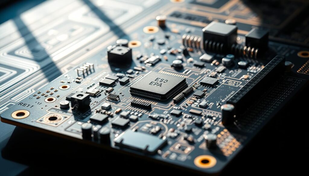
Choosing components with low power requirements is fundamental to designing energy-efficient IoT PCBAs. This involves selecting microcontrollers, sensors, and communication modules that offer a balance between performance and power consumption.
Power Gating and Management Techniques
Implementing power gating and advanced management techniques can significantly reduce consumption in IoT devices. Techniques such as dynamic voltage and frequency scaling (DVFS) and sleep modes help minimize power usage during periods of inactivity.
Battery Selection and Optimization
Battery life is a critical factor in IoT device design. Selecting the right battery type and optimizing its use through intelligent charging and monitoring circuits can extend life and improve overall device reliability. Factors such as energy density, recharge cycles, and environmental conditions influence battery choice.
By adopting these strategies, we can create IoT PCBAs that are not only more energy-efficient but also more reliable and cost-effective over their lifecycle.
Wireless Connectivity Options for IoT PCBAs
As IoT devices become increasingly ubiquitous, selecting the right wireless connectivity option for PCBA design is crucial. We will explore various wireless technologies and their implications for IoT PCBAs.
Short-Range Technologies: Bluetooth LE and Wi-Fi
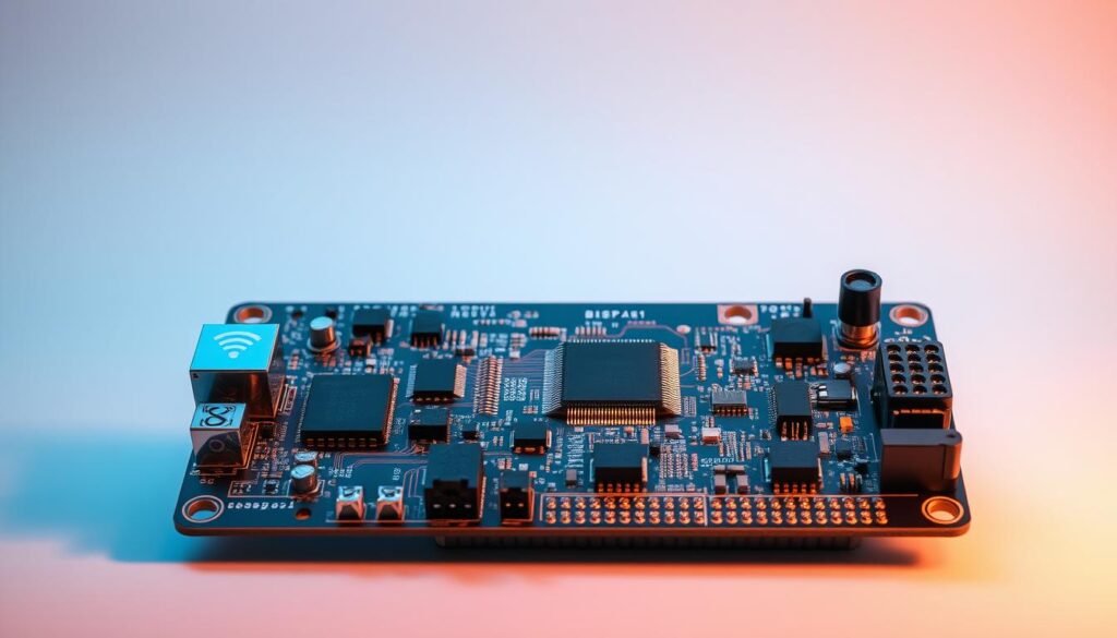
Bluetooth Low Energy (BLE) and Wi-Fi are two prevalent short-range wireless technologies used in IoT applications. BLE is ideal for low-power, low-data-rate applications, while Wi-Fi is suited for high-data-rate applications. Both technologies play a significant role in IoT communication and data transfer.
Long-Range Technologies: LoRaWAN and Cellular
For IoT applications that require long-range connectivity, LoRaWAN and Cellular technologies are employed. LoRaWAN is a low-power, wide-area network technology that operates in unlicensed frequency bands, making it suitable for outdoor IoT deployments. Cellular technologies, such as LTE-M and NB-IoT, utilize existing cellular networks, providing wide-area connectivity for IoT devices that require always-on connectivity and remote operation. These technologies enhance the performance and system reliability of IoT devices.
Antenna Design and Placement Considerations
Antenna design and placement are critical factors that impact the communication range, reliability, and power efficiency of IoT devices. Considerations include:
- PCB trace antennas can reduce component costs but require precise design and controlled impedance.
- External or chip antennas may offer superior performance but need careful integration and matching networks.
- Antenna placement must consider potential sources of interference from other components and nearby objects.
By carefully designing and placing antennas, IoT devices can achieve reliable data transfer and efficient technology utilization in various applications.
How to Design PCBAs for IoT Sensors and Gateways
To effectively design PCBAs for IoT applications, it’s crucial to understand the interplay between sensor integration, signal processing, and gateway design considerations. We will explore these critical aspects in detail.
Sensor Selection and Integration
Selecting the right sensors is fundamental to IoT device functionality. We must consider factors such as accuracy, response time, and environmental conditions. Sensor integration involves connecting these sensors to the PCBA, ensuring compatibility and optimal performance.
Signal Conditioning and Processing
Implementing appropriate signal conditioning circuits is vital to amplify, filter, or convert sensor signals to a suitable form for processing by the microcontroller. This may include amplifiers, analog-to-digital converters (ADCs), or signal conditioning ICs. Effective signal processing enables accurate data interpretation.
Gateway-Specific Design Considerations
IoT gateways require more robust processing capabilities and multiple communication interfaces. Key considerations include supporting concurrent wireless technologies, managing power design for continuous operation, and incorporating security hardware such as secure elements or trusted platform modules (TPMs).
| Design Consideration | Description | Importance |
|---|---|---|
| Sensor Integration | Connecting sensors to PCBA | High |
| Signal Conditioning | Amplifying and filtering sensor signals | High |
| Gateway Design | Robust processing and multiple interfaces | Critical |
Security Implementation in IoT PCBAs

Implementing robust security measures in IoT PCBAs is crucial for protecting sensitive data and ensuring the reliability of IoT devices. We must consider multiple aspects of security to safeguard these devices from various threats.
Hardware-Based Security Features
Hardware-based security features are essential for providing a secure foundation for IoT devices. These features include Trusted Platform Modules (TPMs) and secure cryptoprocessors, which can handle cryptographic operations and store sensitive information securely. By integrating these features into IoT PCBAs, we can significantly enhance their security posture.
Secure Boot and Firmware Protection
Secure boot mechanisms and firmware protection are critical for preventing unauthorized access and ensuring the integrity of IoT device firmware. We can achieve this through secure boot protocols that verify the authenticity of firmware before it is executed. Additionally, firmware protection techniques, such as encryption and secure storage, can further safeguard against tampering and unauthorized access.
Tamper Detection and Prevention
Tamper detection and prevention mechanisms are vital for identifying and responding to physical attacks on IoT devices. Techniques include implementing tamper switches, mesh shields, and environmental sensors to detect tampering attempts. When tampering is detected, the device can be configured to take appropriate actions, such as erasing sensitive data or disabling functionality, to protect itself and its stored information. For more information on IoT security, visit our blog post on IoT security tips.
Testing and Manufacturing Considerations
As we move towards the production phase of IoT PCBAs, it’s crucial to consider testing and manufacturing aspects. Ensuring that IoT devices are reliable and meet the required standards is paramount for their successful deployment.
Functional and Power Consumption Testing
Functional testing verifies that IoT PCBAs operate as intended, while power consumption testing ensures that devices meet the required energy efficiency standards. We must perform thorough testing to identify any potential issues before mass production.
Design for Manufacturing (DFM) Guidelines
Implementing DFM guidelines is essential to streamline the manufacturing process. This includes designing PCBAs with manufacturability in mind, such as optimizing component placement and ensuring sufficient spacing between components.
Quality Control and Compliance Standards
Quality control processes, including automated optical inspection (AOI) and X-ray inspection, help detect manufacturing defects. Moreover, IoT PCBAs must comply with relevant industry standards, such as FCC, CE, or UL certifications, to ensure regulatory compliance.
| Quality Control Measure | Purpose |
|---|---|
| Automated Optical Inspection (AOI) | Detect manufacturing defects such as misaligned components or solder bridges |
| X-ray Inspection | Identify hidden defects like insufficient connections |
| Regulatory Compliance Testing | Verify compliance with standards for EMC, RF emissions, and safety |
Conclusion
IoT PCBA design is a multifaceted process that requires balancing various factors, including power efficiency, connectivity, security, and manufacturability. As we have discussed, selecting the right components, implementing effective power management, and ensuring robust wireless connectivity are crucial for creating reliable IoT devices.
The rapidly evolving IoT technology landscape demands that designers stay abreast of emerging trends, such as edge computing and AI integration, to remain competitive. Collaboration between hardware engineers, firmware developers, and manufacturing specialists is essential for successful IoT PCBA design.
By working with experienced PCBA manufacturing partners, you can improve product quality, reduce time-to-market, and ensure competitive pricing. As IoT applications expand across industries, from consumer electronics to industrial automation, the demand for specialized PCBA design expertise continues to grow. Request an IoT PCBA instant quote today to transform your innovative IoT concept into a manufacturable reality.
FAQ
What are the key considerations when selecting components for IoT PCBAs?
How do I optimize power efficiency in my IoT device’s PCBA?
What wireless connectivity options are available for IoT PCBAs?
What are the most important security features to implement in IoT PCBAs?
What testing and validation procedures should I perform on my IoT PCBA?
What are the benefits of using a printed circuit board assembly (PCBA) manufacturer that follows quality control and compliance standards?
About The Author
Elena Tang
Hi, I’m Elena Tang, founder of ESPCBA. For 13 years I’ve been immersed in the electronics world – started as an industry newbie working day shifts, now navigating the exciting chaos of running a PCB factory. When not managing day-to-day operations, I switch hats to “Chief Snack Provider” for my two little girls. Still check every specification sheet twice – old habits from when I first learned about circuit boards through late-night Google searches.
