When it comes to electronics manufacturing, ensuring the quality and reliability of PCBs is crucial. Testing each PCB individually can be a time-consuming and costly process, especially for complex electronics. We often find ourselves wondering if there’s a more efficient way to verify that our PCBs meet design specifications.
A test jig, also known as a fixture, is a mechanical and electronic apparatus designed to assess a product at various levels. By utilizing a custom test jig, manufacturers can significantly streamline the PCBA testing process, reducing testing time from hours to just minutes per board.
Key Takeaways
- Streamline PCBA testing with custom test jigs, reducing testing time.
- Ensure PCB quality and reliability with functional testing.
- Save thousands of dollars by identifying defects early.
- Understand the test jig development process from planning to validation.
- Learn industry best practices for creating effective test jigs.
Understanding Test Jigs and Their Importance
To guarantee the reliability and performance of PCBA, manufacturers rely on test jigs that enable precise and efficient testing. A PCBA test fixture, also known as a jig, is a custom-made device designed to operate electrical and functional testing on the PCBA after the electronic components have been surface-mounted and through-hole mounted on the board.
What is a Functional Test Jig?
A functional test jig uses a physical interface, such as spring pins and sockets, to connect to the PCBA for testing. It achieves automatic or half-automatic testing to increase PCBA testing accuracy and efficiency. By using PCBA test fixtures, the PCBA manufacturer can prevent human test errors and ensure test consistency.
Benefits of Custom Test Jigs in PCBA Manufacturing
The benefits of using custom test jigs in PCBA manufacturing are multifaceted. They create a controlled environment for evaluating printed circuit board assemblies under conditions that simulate real-world usage. This not only enhances the reliability of the testing process but also bridges the gap between design validation and volume manufacturing by providing consistent, repeatable test results.
| Benefits | Description |
|---|---|
| Increased Testing Accuracy | Automatic or half-automatic testing reduces human error |
| Improved Efficiency | Streamlined testing process for PCBA |
| Consistent Test Results | Ensures reliability and performance of PCBA |
By understanding the role and importance of test jigs, manufacturers can significantly improve their PCBA testing processes, leading to higher quality products and reduced production costs.
Essential Components of a Custom Test Jig for FCT
When designing a custom test jig for Functional Circuit Test (FCT), several essential components must be considered to ensure effective testing. A well-designed test jig is crucial for the reliable testing of Printed Circuit Board Assemblies (PCBA).
Bed of Nails PCB Design
The bed of nails PCB design is a critical component that serves as the primary interface between the test system and the device under test. It is typically designed by the same person who designed the PCB being tested, ensuring that the test points on the PCB align with the bed of nails fixture.
The bed of nails PCB is usually identical in size to the PCB being tested and has holes for nails instead of test pads at the same positions. This design enables reliable contact with the test points on the PCB.
Clamp Mechanism and Mechanical Structure
A clamp mechanism is used to apply pressure on the PCB so that the bed of nails can make good contact with the test points. The main body of the jig, which can be sourced from various suppliers or custom-built, houses the clamp mechanism and other components.
Designing an effective clamp mechanism requires careful consideration of mechanical factors to ensure consistent pressure and alignment during testing.
Control Systems and Interfaces
Control systems are necessary for automated testing, including microcontrollers, relays, and interface electronics. These components work together to control the test process and communicate with the host computer.
Common communication protocols used between test fixtures and host computers include USB, UART, and CAN. The choice of protocol depends on the specific requirements of the test system.
Optional Components for Enhanced Testing
Several optional components can enhance the capabilities of a custom test jig, including displays for user feedback, printers for test reports, and specialized measurement equipment. These components can be integrated based on the specific needs of the test process.
When selecting components, it’s essential to consider factors such as budget and production volume requirements to ensure the test jig is cost-effective and efficient.
Designing Your Custom Test Jig Step-by-Step
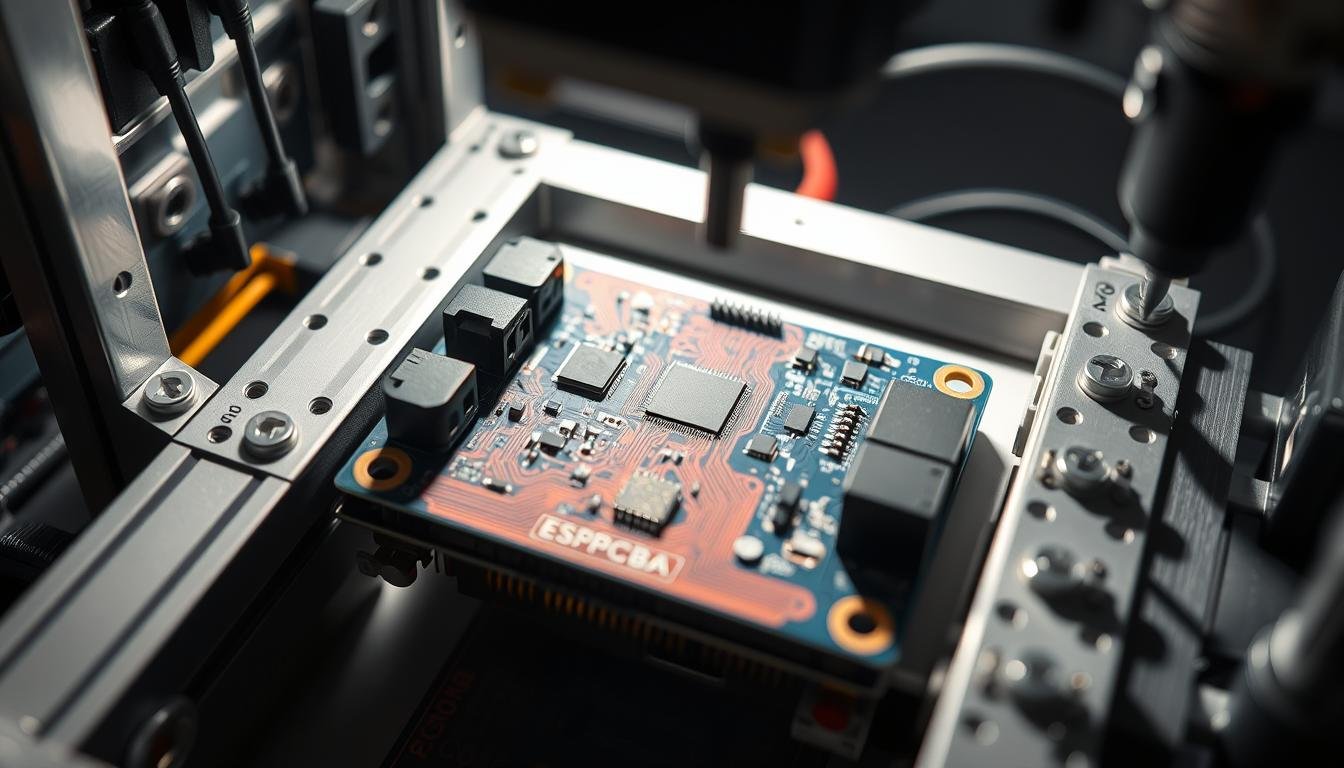
 with numerous test points, showcasing the ESPCBA brand. The PCB surface is illuminated with a soft, directional light from the top left, casting subtle shadows and highlighting the intricate copper traces and solder pads. The test points are prominently featured, displaying their precise, circular design and arranged in a visually appealing, organized layout. The background is slightly blurred, emphasizing the technical focus on the PCB components. The overall mood is one of precision, functionality, and the attention to detail required in the design and testing of electronic circuits.")
The process of designing a custom test jig for FCT involves several key steps that, when followed, ensure the jig meets the required testing standards. We will guide you through these steps, providing insights into best practices for PCB testing and design.
Planning Test Points on Your PCBA
Effective test point planning is crucial for efficient testing. To optimize testing efficiency, think modularly and focus on key testing points based on potential failure and key features that need to be tested. For instance, using a test point to measure current or detect voltage if an LED is on or off is not really efficient. LEDs have low failure rates and are often tied to other components, making them less critical for individual testing. Prioritize test points that verify critical circuit functions.
When placing test points, ensure they are at least 2 mm apart and positioned on a single side of the PCB. Test points should be at least 1 mm in diameter, with 2.5 mm being a common standard. Avoid stacking all test points on one side of the board to maintain accessibility and reliability.
Creating the Mechanical Fixture
Designing the mechanical fixture involves considerations for alignment pins, pressure distribution, and ergonomic operation. The fixture should securely hold the PCBA in place, ensuring reliable contact between test probes and test points. A well-designed mechanical fixture enhances the overall efficiency of the test process.
Developing the Test Point Carrier Board
The Test Point Carrier Board (TPCB) interfaces between your test probes and instrumentation. Developing a TPCB requires careful consideration of signal integrity and routing to ensure accurate test results. This component is crucial for the effective operation of your custom test jig.
Integrating Test Instrumentation
Selecting and integrating appropriate test instrumentation is based on your specific measurement requirements. This step involves choosing the right tools for the job, ensuring that your test jig can perform the necessary tests accurately and efficiently. The integration of test instrumentation completes the test system, enabling comprehensive testing of your PCBA.
By following these steps and considering the guidelines provided, you can design a custom test jig that meets your specific testing needs, enhancing the efficiency and reliability of your PCBA functional test process.
Implementing Firmware and Test Software

The success of your functional test depends on the effective implementation of firmware and test software. When developing a custom test jig for PCBA testing, it’s crucial to consider both aspects to ensure comprehensive testing and reliable results.
Choosing the Right Firmware Approach
There are two primary approaches to test firmware implementation: dedicated test firmware and embedded test routines in production firmware. Dedicated test firmware involves loading specific firmware designed for testing, which is then replaced with the actual firmware if the unit passes all tests. On the other hand, embedding test routines directly into your firmware allows the test jig to execute these tests. The latter approach has distinct advantages, including ensuring that no unit leaves the floor with the wrong firmware loaded and contributing to comprehensive firmware testing.
Test Software Options
The choice of test software is critical for developing and running functional tests. Popular options include National Instruments LabVIEW and TestStand, which are widely used for their ease of use with PXI Instrumentation. However, they can be challenging to configure with non-NI test instrumentation. LabVIEW is a programming language used to write functional tests, offering a robust platform for test development. Alternatively, open-source test software platforms can provide a cost-effective solution, although they may require more development effort.
Creating Effective Test Procedures
Developing effective test procedures is essential for balancing thoroughness with testing efficiency. This involves structuring test sequences to quickly identify common failure modes while maintaining comprehensive coverage. Automated pass/fail criteria can reduce subjective interpretation of test results, enhancing the reliability of the testing process. Additionally, considerations for data logging and reporting facilitate quality tracking and continuous improvement.
Conclusion: Maximizing the Value of Your Custom Test Jig
As we conclude our exploration of custom test jigs for functional testing, it’s clear that these specialized tools offer significant advantages in PCBA manufacturing. By implementing a well-designed test jig, you can improve the quality and efficiency of your PCBA functional testing process.
The benefits of custom test fixtures extend beyond initial cost savings. They provide long-term value by adapting to your evolving products and manufacturing process. The data collected through functional testing drives continuous improvement in both product design and manufacturing processes.
To maximize the value of your custom test jig, it’s essential to maintain and update it as your products evolve or production volumes increase. Proper documentation and knowledge transfer ensure your test system remains valuable even as team members change. By investing in quality functional testing, you can ultimately achieve higher customer satisfaction and reduced warranty claims.
For organizations looking to implement or improve their functional test capabilities, we recommend partnering with experienced test fixture designers to accelerate your path to effective functional testing. By working with a one-stop PCBA manufacturer like PCBONLINE, you can streamline your testing and inspection processes. To get a quote from PCBONLINE, contact info@pcbonline.com.