Ensuring the quality of PCB assembly is crucial in electronics manufacturing. The question is, are you using the right inspection method? Automated Optical Inspection (AOI) and Automated X-ray Inspection (AXI) are two popular options, each with unique advantages. While AOI excels at detecting surface-level defects like component placement and solder issues, AXI penetrates deeper to reveal hidden connections and internal defects, such as those in Ball Grid Arrays (BGAs).
As PCBs become increasingly complex with dense component packaging, the importance of AXI technology grows. It provides manufacturers with complete confidence in their PCB assemblies by identifying defects that AOI cannot.
Key Takeaways
- Understand the critical differences between AOI and AXI technologies.
- Learn how AXI detects hidden defects in PCB assemblies.
- Discover why AXI is essential for comprehensive PCB quality assurance.
- Determine when to implement AXI and when AOI is sufficient.
- Develop an optimal inspection strategy for your manufacturing needs.
Understanding PCB Inspection Technologies
The landscape of PCB manufacturing has been revolutionized by advancements in inspection technologies. As we continue to push the boundaries of electronics manufacturing, the role of inspection in ensuring quality and reliability has become increasingly critical.
The Critical Role of Inspection in PCB Manufacturing
Inspection is a cornerstone of PCB manufacturing, enabling the detection of defects that could compromise the integrity of the final product. Automated Optical Inspection (AOI) and Automated X-Ray Inspection (AXI) are two pivotal technologies that have transformed the inspection process. AOI uses high-resolution cameras and sophisticated lighting to scan PCBs for surface-level defects, comparing captured images against a ‘golden standard’ to identify discrepancies.
Evolution of Automated Inspection Methods
The journey of PCB inspection has been marked by significant milestones, from simple visual checks to sophisticated automated systems capable of detecting microscopic defects. Key developments include the introduction of automated optical inspection systems in the 1980s and automated x-ray inspection technology in the 1990s. Today’s inspection equipment combines multiple technologies, including 3D imaging, artificial intelligence, and machine learning, to achieve unprecedented accuracy and speed.
| Inspection Technology | Key Features | Benefits |
|---|---|---|
| Automated Optical Inspection (AOI) | High-resolution cameras, sophisticated lighting | Surface-level defect detection, high accuracy |
| Automated X-Ray Inspection (AXI) | X-Ray technology, 2D and 3D imaging | Detection of hidden defects, inspection of complex components |
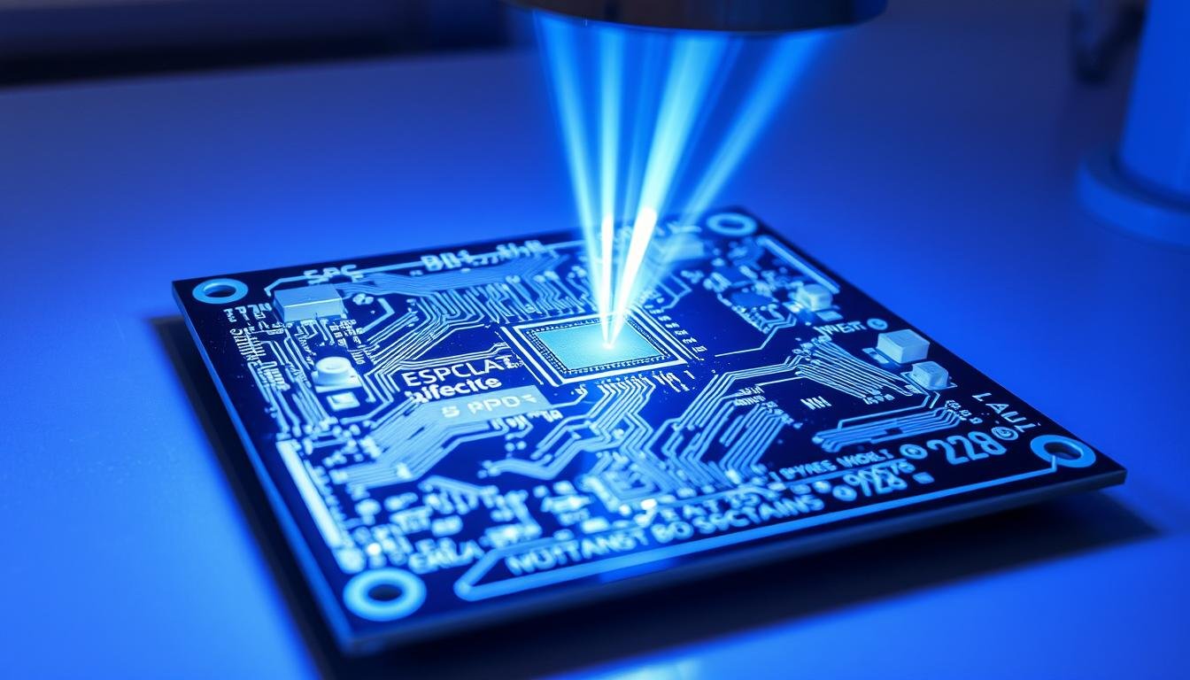
Automated Optical Inspection (AOI): Capabilities and Limitations
 system, meticulously examining a complex printed circuit board (PCB) under bright, directional lighting. Precisely calibrated high-resolution cameras capture every minute detail, scrutinizing solder joints, component placement, and surface-mount technology features. In the foreground, a digital display showcases real-time analysis, highlighting any anomalies or defects with color-coded indicators. The middle ground reveals the intricate PCB layout, with delicate copper traces and numerous electronic components. The background fades into a clean, clinical environment, emphasizing the technology's precision and the importance of quality control in modern electronics manufacturing.")
The use of AOI in PCB manufacturing has revolutionized the inspection process, enabling the detection of surface-level defects with high accuracy. We leverage AOI technology to ensure the quality of our PCBs by inspecting for visible defects that could impact their performance.
How AOI Technology Works
AOI systems utilize cameras and sophisticated software to inspect the surface of circuit boards. They capture high-resolution images of the PCB and compare them against predefined standards to identify defects. This process allows for the detection of issues such as missing components, misaligned parts, and solder defects.
Types of Defects AOI Can Detect
AOI is effective in detecting a variety of surface-level defects, including component absence, incorrect component orientation, and solder bridging. By identifying these issues, manufacturers can correct problems early in the production process, reducing waste and improving overall efficiency.
| Defect Type | Description | Impact on PCB |
|---|---|---|
| Component Absence | Missing components on the PCB | Functional failure |
| Solder Bridging | Excess solder connecting pins | Short circuits |
| Misaligned Components | Components not correctly positioned | Performance issues |
Limitations of Surface-Level Inspection
While AOI is highly effective for surface defects, it has significant limitations. It cannot inspect internal layers or hidden solder joints, such as those under BGA packages. Additionally, tall components can obstruct the view of shorter ones, creating blind spots. We also recognize that AOI may flag acceptable variations as defects, slowing production.
Advanced X-Ray Inspection (AXI): What It Reveals That AOI Cannot

AXI technology has revolutionized the way we inspect PCBs, providing a detailed look at solder joints and internal structures. While Automated Optical Inspection (AOI) is excellent for detecting surface-level defects, AXI fills the gap by focusing on internal and hidden defects.
X-Ray Technology in PCB Inspection
X-ray technology is pivotal in inspecting the internal structures of PCBs, particularly for complex components like Ball Grid Arrays (BGAs) and Chip Scale Packages (CSPs). X-ray inspection allows us to visualize solder joints that are not visible through optical means.
2D vs. 3D X-Ray Inspection
There are two primary types of X-ray inspection: 2D and 3D. 2D X-ray inspection provides a two-dimensional view, useful for initial assessments and simpler PCBs. In contrast, 3D X-ray inspection offers a more detailed, three-dimensional view, crucial for complex, multilayer PCBs where defects can be hidden in multiple layers.
Critical Hidden Defects Only AXI Can Detect
AXI is particularly adept at detecting several critical defects that are invisible to AOI, including:
- BGA and CSP Solder Joint Inspection: AXI can identify voids, insufficient solder, or bridging in these hidden connections.
- Solder Voids Detection: Gas pockets within solder joints that can compromise thermal performance and reliability.
- Head-in-Pillow Defects: Incomplete contact between solder paste and component terminations, leading to weak connections.
- Insufficient Barrel Fill in PTH Holes: Ensuring solder penetration meets the required standards for Class 3 electronics.
- Internal PCB Layer Cracks and Delamination: Structural defects that can lead to intermittent failures under stress.
By leveraging AXI, manufacturers can significantly enhance the quality and reliability of their PCB assemblies. It’s a powerful tool in the fight against defects that are otherwise invisible, ensuring that PCBs perform as intended, even in the most demanding applications.
Key Differences Between AOI and AXI
 inspection station featuring the ESPCBA brand. The scene depicts a sophisticated laboratory environment with state-of-the-art x-ray scanning equipment, robotic manipulators, and a large display panel showcasing the PCB's internal structure. Precise lighting from multiple angles accentuates the intricate copper traces, vias, and component placements. In the foreground, a technician in a clean-room suit carefully examines the PCB, while the background showcases other inspection tools and workstations. The overall atmosphere conveys a sense of advanced technology, precision, and quality control essential for modern electronic manufacturing.")
When it comes to PCB inspection, understanding the differences between AOI and AXI is crucial for manufacturers. The distinction between these two technologies lies in their inspection approaches, defect detection capabilities, and operational considerations.
Technology and Inspection Approach
AOI uses optical cameras to capture images of the PCB surface, inspecting for defects based on visual criteria. In contrast, AXI employs X-ray technology to examine the internal structures of components and solder joints, providing a more comprehensive inspection.
Defect Detection Capabilities
While AOI is effective at detecting surface-level defects such as solder bridging, insufficient solder, and component misalignment, AXI excels at identifying hidden defects within components and complex solder joints, such as those found in BGA packages.
Speed, Throughput, and Cost Considerations
AOI systems are generally faster, inspecting PCBs in 10-20 seconds, making them suitable for high-volume production. AXI systems are slower, taking 30-60 seconds or more per board, especially for detailed 3D X-ray scans. The cost also varies significantly, with AOI systems starting at around $50,000 and AXI systems beginning at $100,000, reaching up to $500,000 for advanced 3D X-ray models.
We observe that the choice between AOI and AXI depends on the specific needs of the production line, including the type of components used, the required inspection speed, and the budget for equipment and maintenance.
- AOI is ideal for high-volume production environments where speed is critical.
- AXI is better suited for applications requiring detailed inspection of internal component structures.
- The total cost of ownership for AXI systems is higher due to specialized maintenance and energy consumption.
When to Choose AXI Over AOI
In the realm of PCB inspection, AXI emerges as a critical technology for applications where hidden defects can have catastrophic consequences. As we navigate the complexities of modern electronics manufacturing, understanding when to opt for AXI over AOI is crucial for ensuring the quality and reliability of pcb assembly products.
Complex Component Packages (BGA, CSP, QFN)
Complex component packages such as Ball Grid Arrays (BGA), Chip Scale Packages (CSP), and Quad Flat No-leads (QFN) pose significant inspection challenges due to their hidden solder joints. AXI is particularly adept at inspecting these components, providing a detailed view of the solder joints that are not visible to AOI systems. This capability is essential for detecting defects like solder voids, insufficient solder, or misaligned components that can lead to failures in circuit board assemblies.
High-Reliability Applications (Aerospace, Medical, Automotive)
For industries with strict reliability standards, such as automotive, aerospace, or medical, AXI is often non-negotiable. Defects like solder voids or internal cracks can lead to catastrophic failures, and AXI’s ability to detect these issues ensures compliance with standards like IPC-A-610. The table below highlights key industries and their inspection requirements:
| Industry | Inspection Requirements | Standards Compliance |
|---|---|---|
| Aerospace | Comprehensive inspection protocols | AS9100 |
| Medical | Risk management emphasis | FDA regulations, ISO13485 |
| Automotive | Exceptional solder joint integrity | IPC-A-610 |
By choosing AXI, manufacturers can ensure the quality of their products and compliance with industry standards, ultimately justifying the additional production time and expense of comprehensive X-ray inspection.
Implementing a Hybrid Inspection Strategy
To maximize defect detection and minimize production downtime, a hybrid inspection strategy is essential. This approach combines the strengths of both Automated Optical Inspection (AOI) and Advanced X-Ray Inspection (AXI) to ensure comprehensive quality control throughout the PCB assembly process.
Complementary Use of AOI and AXI
AOI and AXI serve different but complementary roles in the inspection process. While AOI excels at detecting surface-level defects, AXI provides critical insights into internal structures and hidden defects. By integrating both technologies, manufacturers can achieve a more thorough inspection process. We recommend using AOI for initial defect detection and AXI for verifying complex assemblies or high-reliability products. For more information on choosing the right inspection method, visit our detailed guide on AOI vs. AXI.
Strategic Placement in the Production Line
Strategic placement of inspection equipment within the production line significantly impacts both defect detection effectiveness and manufacturing throughput. We typically recommend positioning AOI systems at multiple points—after solder paste printing, after component placement, and after reflow. AXI equipment is best utilized either as an offline sampling station for high-volume products or as an end-of-line verification for high-reliability assemblies. For mixed production environments, configuring a flexible routing system allows boards with complex components to be diverted to AXI inspection while simpler assemblies proceed directly through AOI.
Future Trends in PCB Inspection Technology
As we look to the future, PCB inspection technology is poised to undergo significant advancements. The integration of AI and machine learning is set to play a crucial role in enhancing inspection capabilities.
AI and Machine Learning Integration
We are witnessing a significant shift towards the integration of AI and machine learning in PCB inspection. This trend is enabling more sophisticated defect detection and classification. By leveraging advanced algorithms, manufacturers can improve inspection accuracy and reduce false calls. For more information on how X-ray inspection systems are used in PCB manufacturing, visit our comprehensive guide.
Advancements in X-Ray Technology
X-ray inspection technology is advancing rapidly, with developments in 3D X-ray imaging and computed tomography (CT) providing more detailed views of internal structures. New digital detectors offer higher resolution and faster image acquisition, reducing AXI cycle times by up to 50%. These advancements are making AXI more viable for inline use in high-volume settings.
The trend is towards smarter, integrated inspection systems that combine AOI and AXI data into a single platform, offering a holistic view of PCB quality. This integration enables manufacturers to make more informed decisions and improve overall quality.
Conclusion: Making the Right Inspection Choice for Your PCB Assembly Needs
Ultimately, the decision to use AOI, AXI, or both, hinges on understanding the strengths and limitations of each inspection method. By considering your specific product requirements, reliability expectations, and production volume, you can tailor your inspection strategy to ensure high-quality PCB assembly.
We emphasize that there is no one-size-fits-all solution; the optimal approach must balance detection capabilities against throughput requirements and budget constraints. For complex assemblies with hidden interconnections, AXI provides critical quality assurance, while AOI may suffice for simpler surface-mount components.
As your products evolve, so should your inspection strategy, adapting to maintain comprehensive defect detection capabilities. Investing in the right inspection technology ultimately enhances your brand reputation and reduces field failures.