Can a single faulty circuit bring down an entire electronic system? The answer is often yes, and it’s a scenario that engineers strive to avoid. Printed Circuit Boards (PCBs) are the backbone of modern electronics, powering everything from smartphones to industrial machinery.
However, even the most meticulously designed PCBs can fail, leading to costly downtime or complete device failure. Understanding the root causes of these failures is critical for ensuring reliability and longevity in designs.
We will explore the importance of identifying and resolving open circuits and other issues that disrupt current flow. By applying systematic analysis techniques, engineers can diagnose and address underlying problems rather than just treating symptoms.
Key Takeaways
- Understanding the critical importance of root cause analysis in PCBA failures.
- A systematic approach to diagnosing common PCBA failures.
- Improving manufacturing processes and product reliability through failure analysis.
- Basic and advanced analytical techniques for revealing hidden defects.
- Practical knowledge for implementing effective troubleshooting protocols.
- Transforming quality control processes based on failure mechanisms.
The Critical Importance of PCBA Failure Analysis
The complexity of modern PCBs necessitates thorough failure analysis to prevent future issues. As electronic circuits become increasingly sophisticated, with high-density interconnects, lead-free soldering, and multi-layer designs, the importance of comprehensive failure analysis cannot be overstated.
Why Failure Analysis Matters in Electronics Manufacturing
Failure analysis is crucial in electronics manufacturing as it helps identify the root causes of PCBA failures, enabling manufacturers to address quality issues and improve their production processes. By doing so, companies can reduce the number of failures and associated costs, ultimately enhancing their bottom line.
The Cost of Unresolved PCBA Failures
Unresolved PCBA failures can have far-reaching consequences, including production downtime, shipping delays, and damaged customer relationships. Our analysis will quantify the true costs of such failures and demonstrate how investing in proper failure analysis can provide a substantial return on investment through reduced scrap rates, fewer field failures, and extended product lifecycles.
By examining case studies and providing a framework for calculating the comprehensive cost of PCBA failures, we’ll help organizations justify investments in quality assurance and failure analysis capabilities, ultimately improving their overall operational efficiency.
Understanding Common PCBA Failure Modes
Understanding the common failure modes in PCBA is crucial for enhancing the reliability of electronic devices. PCBA failures can occur due to various reasons, including manufacturing defects, design flaws, and environmental factors.
Solder Joint Failures and Their Causes
Solder joint failures are a common issue in PCBA, often resulting from inadequate soldering processes or environmental stresses such as thermal cycling. Poor solder joints can lead to intermittent connections or complete circuit failures. Ensuring proper soldering techniques and material quality is vital for preventing such failures.
Open and Short Circuits in PCBAs
Open and short circuits are significant failure modes in PCBAs. Open circuits occur when there’s a break in the circuit, preventing the flow of current, while short circuits happen when there’s an unintended path for current to flow, often causing damage to components. These issues can arise from manufacturing defects, design errors, or physical damage to the PCB.
Component Failures and Degradation
Components such as resistors, capacitors, and ICs can fail due to electrical overstress, defective parts, or aging. Electrical overstress from overvoltage or overcurrent can burn out components, while low-quality or counterfeit parts may fail prematurely. Components like capacitors may degrade over time, reducing overall PCBA performance and reliability.
Signal Integrity and Environmental Issues
As we delve into the complexities of PCBA failures, it’s crucial to examine the dual challenges of signal integrity and environmental issues. High-speed PCBAs are particularly susceptible to signal integrity problems, which can lead to data corruption and system failures.
Signal Integrity Problems in High-Speed PCBAs
Signal integrity issues in high-speed PCBAs arise from factors such as impedance mismatches, crosstalk, and signal attenuation. These problems can be exacerbated by poor design practices, inadequate shielding, and improper routing techniques. To mitigate these issues, designers must employ careful planning and advanced simulation tools to ensure signal integrity.
Environmental Damage and Its Impact
Environmental factors such as moisture, temperature extremes, and contamination can significantly impact PCBA reliability. For instance, high humidity levels can lead to corrosion or conductive anodic filament (CAF) formation, while operating beyond a PCB’s rated temperature can cause warping or material degradation.
| Environmental Factor | Impact on PCBA |
|---|---|
| High Humidity | Corrosion, CAF formation |
| Temperature Extremes | Warping, material degradation |
| Contamination | Shorts, corrosion, insulation resistance failures |
By understanding these environmental challenges and implementing protective strategies such as conformal coatings and specialized board materials, we can enhance the reliability and longevity of PCBAs in harsh environments.
Essential Tools for Root Cause Analysis
 undergoing comprehensive analysis. In the foreground, a dissected ESPCBA board with intricate copper traces, vias, and components exposed, illuminated by warm, focused lighting. The middle ground showcases precision measurement tools like multimeters and logic analyzers examining the board, conveying a sense of meticulous investigation. In the background, a complex schematic diagram or x-ray view of the PCB's inner layers provides additional context. The overall scene exudes an atmosphere of methodical analysis, engineering expertise, and a quest to uncover the root causes of potential failures.")
To conduct a thorough root cause analysis, we rely on a range of essential tools that help us identify and understand PCBA failures. These tools are crucial in enabling us to diagnose issues accurately and implement corrective actions.
Visual Inspection Equipment
Visual inspection equipment is fundamental in identifying surface-level defects and anomalies in PCBAs. We use high-resolution cameras and microscopes to examine components, solder joints, and PCB surfaces for signs of damage or irregularities. This visual inspection is often the first step in the analysis process, helping us to quickly identify potential causes of failure.
Electrical Testing Instruments
Electrical testing instruments are vital for assessing the electrical performance of PCBAs. We employ tools such as multimeters, oscilloscopes, and signal generators to measure voltage, current, and signal integrity. These instruments help us to identify electrical faults, such as open or short circuits, and to verify that components are functioning within specified parameters.
Advanced Imaging Technologies
Advanced imaging technologies play a critical role in examining the internal structures of PCBAs without causing damage. Techniques such as non-destructive X-ray imaging and computed tomography (CT) scanning allow us to inspect solder joints, vias, and other internal features. Additionally, scanning electron microscopy (SEM) provides high-resolution images and elemental analysis, helping us to study microstructural defects and contamination.
| Tool | Application | Benefits |
|---|---|---|
| X-ray Imaging | Inspecting internal structures like solder joints and vias | Non-destructive, detailed visualization |
| SEM | High-resolution imaging and elemental analysis | Detailed defect analysis, contamination detection |
| CT Scanning | Creating 3D models of PCBAs | Comprehensive internal examination |
Root Cause Analysis for Common PCBA Failures: Step-by-Step Approach
In our experience, a thorough root cause analysis is essential for understanding and mitigating common PCBA failures. By understanding failure modes and their origins, engineers can improve design reliability, reduce rework, and enhance product performance.
Initial Assessment and Documentation
The first step in root cause analysis involves a thorough initial assessment and meticulous documentation of the failure. This includes gathering data on the failure mode, environmental conditions, and any other relevant factors. We emphasize correlation between electrical measurements, visual observations, and environmental factors to establish causal relationships.
Systematic Testing Procedures
Systematic testing procedures are critical for identifying the root cause of PCBA failures. We design and implement confirmation tests that verify suspected root causes by reproducing the failure under controlled conditions, often related to open circuits or open circuit issues.
Data Analysis and Failure Confirmation
During data analysis, we synthesize data from multiple test methods to build a comprehensive understanding of the failure mechanism. Statistical analysis techniques help identify patterns that point to systematic issues rather than random failures, ensuring that corrective actions address fundamental issues rather than secondary effects.
| Step | Description | Outcome |
|---|---|---|
| Initial Assessment | Gather data on failure mode and conditions | Identify potential causes |
| Systematic Testing | Design and implement confirmation tests | Verify suspected root causes |
| Data Analysis | Synthesize data from multiple test methods | Understand failure mechanism |
Visual Inspection Techniques for PCBA Troubleshooting
 undergoing visual inspection. The ESPCBA board is positioned at a slight angle, allowing for a clear view of its intricate copper traces, solder joints, and component placements. Bright, evenly distributed lighting illuminates the scene, casting subtle shadows that accentuate the board's topology. The image is captured with a high-resolution camera lens, rendering the PCB's features with exceptional clarity and precision. The overall mood is one of focused analysis, inviting the viewer to examine the board's condition and identify potential issues or anomalies.")
Visual inspection techniques stand at the forefront of PCBA failure analysis, offering immediate insights into potential issues. We employ a range of methods to identify defects and anomalies in PCBAs.
Surface-Level Inspection Methods
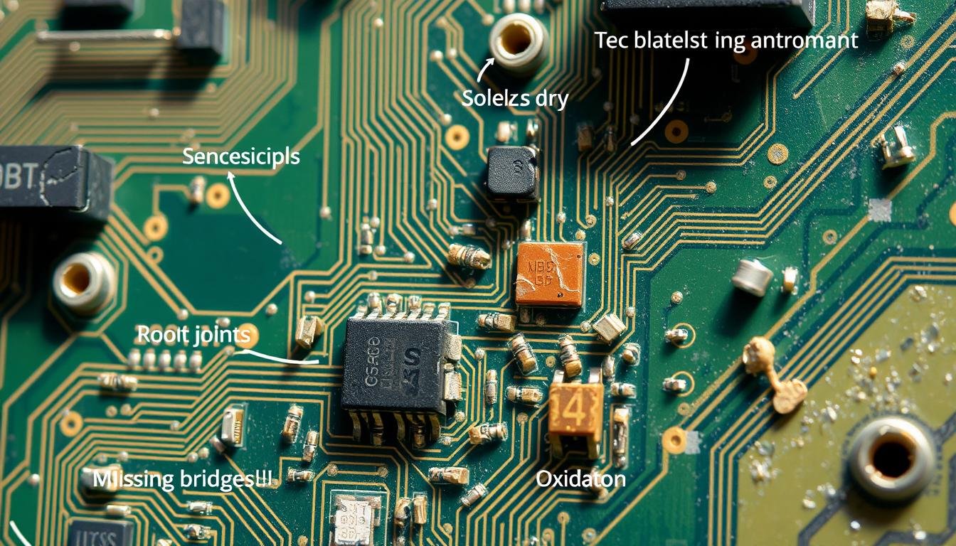
Surface-level inspection is the initial step in PCBA troubleshooting. It involves a thorough examination of the PCB assembly’s surface to identify visible defects such as solder bridges, component misalignment, or signs of physical damage. Effective surface-level inspection can reveal issues that may cause or contribute to PCBA failures. For instance, a visual inspection might reveal a solder bridge between two 0.4 mm-pitched pins, causing a short circuit.
Microscopic Examination Procedures
For more detailed analysis, microscopic examination procedures are utilized. Metallurgical microscopes with higher magnification (up to 1000x) are used to identify micro-cracks or contamination that are not visible to the naked eye. Our microscopy approach emphasizes the importance of proper sample preparation, including cleaning procedures that remove obscuring contaminants without disturbing evidence of failure mechanisms.
| Microscopic Examination Techniques | Description | Benefits |
|---|---|---|
| Digital Microscopy | Extended depth-of-field capabilities | Overcomes limitations of conventional microscopes |
| Sample Preparation | Cleaning procedures | Removes contaminants without disturbing evidence |
By combining surface-level inspection with microscopic examination procedures, we can comprehensively analyze PCBA failures and identify root causes.
Advanced Analytical Methods for Complex Failures
Advanced analytical methods play a vital role in diagnosing complex PCBA failures. These techniques provide detailed insights into the internal structures and interfaces of PCBAs, enabling manufacturers to identify and address failures effectively.
X-Ray Inspection for Internal Defects
X-Ray inspection is a critical technique for examining internal defects in PCBAs. It allows for the visualization of internal structures such as solder joints and plated through-holes without damaging the assembly. By using X-Ray inspection, manufacturers can detect issues like voids, cracks, and improper soldering. For more information on analytical technologies, visit Lab Manager.
Scanning Electron Microscopy Applications
Scanning Electron Microscopy (SEM) is another powerful tool used in PCBA failure analysis. SEM provides high-resolution images of the surface topography of components and solder joints, helping to identify defects such as cracks, delamination, and contamination. Its high magnification capabilities make it invaluable for analyzing microscopic failures in complex circuit boards.
Cross-Sectioning Analysis Techniques
Cross-sectioning analysis involves slicing a PCB to examine its internal structures in detail. This destructive technique is used to inspect solder joint quality, plating thickness, and other internal features. For instance, cross-sectioning can reveal a 10 µm crack in a PTH barrel, indicating thermal fatigue. We examine the complete cross-sectioning process, from sample extraction to etching techniques, and discuss how to interpret findings such as plating thickness measurements and void characterization in each layer of the PCB.
Thermal Analysis in PCBA Failure Investigation
We employ thermal analysis as a key tool in diagnosing PCBA failures, providing insights into thermal-related issues that affect circuit performance. Thermal analysis enables us to visualize and understand the thermal behavior of PCBAs under various operating conditions.
Identifying Thermal-Related Failures
Thermal-related failures often manifest due to component overheating, inadequate heat dissipation, or thermal stress. Thermal imaging might reveal a capacitor operating at 160°C, exceeding its 125°C rating, indicating a potential failure cause. To identify such issues, we:
- Conduct thorough thermal analysis to detect hotspots and thermal anomalies.
- Analyze the thermal profile of components to ensure they are within specified operating temperatures.
- Use comparative thermal analysis between known-good boards and failed units to identify anomalous thermal patterns.
Using Thermal Imaging for Diagnosis
Thermal imaging is a powerful diagnostic tool that provides non-contact, real-time visualization of temperature distributions across entire PCBA assemblies. Our thermal imaging methodology emphasizes proper setup, including emissivity calibration, ambient temperature control, and appropriate viewing angle selection, to ensure accurate temperature measurements. We also conduct powered sequential thermal imaging to capture the thermal profile development during startup, normal operation, and under various load conditions.
By interpreting thermal patterns, we can identify potential issues such as current leakage paths, power distribution network inadequacies, and component thermal coupling effects. For production environments, automated thermal imaging systems can be integrated into functional testing to identify potential reliability issues before products leave the factory.
Implementing Preventive Strategies Based on Root Cause Findings
The insights gained from root cause analysis enable us to develop targeted strategies for improving PCBA reliability. By understanding the underlying causes of failures, we can implement effective preventive measures to minimize future occurrences.
Design Improvements to Prevent Recurrence
We can modify the design to address the root causes of failures. For instance, if solder joint failures are common, we can adjust the PCB layout or component placement to reduce stress on these joints. This proactive approach helps prevent recurrence and enhances overall PCBA reliability.
Manufacturing Process Optimization
Thorough testing is crucial in the manufacturing process. This includes in-circuit testing (ICT), functional testing, and burn-in testing to identify potential issues early on. By optimizing these processes, we can reduce the likelihood of failures and minimize production time.
Quality Control Enhancements
Our quality improvement methodology emphasizes defect containment through multi-stage inspection strategies. By focusing inspection and testing resources on critical potential failure points, we can enhance quality control and reduce costs. Effective metrics should be established to measure the occurrence of known failure modes and the effectiveness of implemented quality improvements.
By implementing these preventive strategies, we can significantly improve PCBA reliability and reduce the risk of future failures.
Conclusion: Transforming Failures into Future Reliability
By understanding and addressing the root causes of PCBA failures, we pave the way for future reliability. Our comprehensive approach to root cause analysis has shown that investing time and resources in thorough failure analysis yields substantial returns through enhanced product reliability, reduced warranty costs, and improved customer satisfaction.
We’ve established a framework for a failure analysis culture that views failures as learning opportunities, encouraging transparent reporting and collaborative problem-solving. This culture, combined with advanced analysis techniques, enables organizations to transform their manufacturing operations from reactive to proactive quality assurance.
Ultimately, our analysis demonstrates that effective root cause analysis transforms PCBA failures into valuable opportunities for systemic improvement across design, manufacturing, and quality processes, leading to enhanced quality and reduced circuit failures.