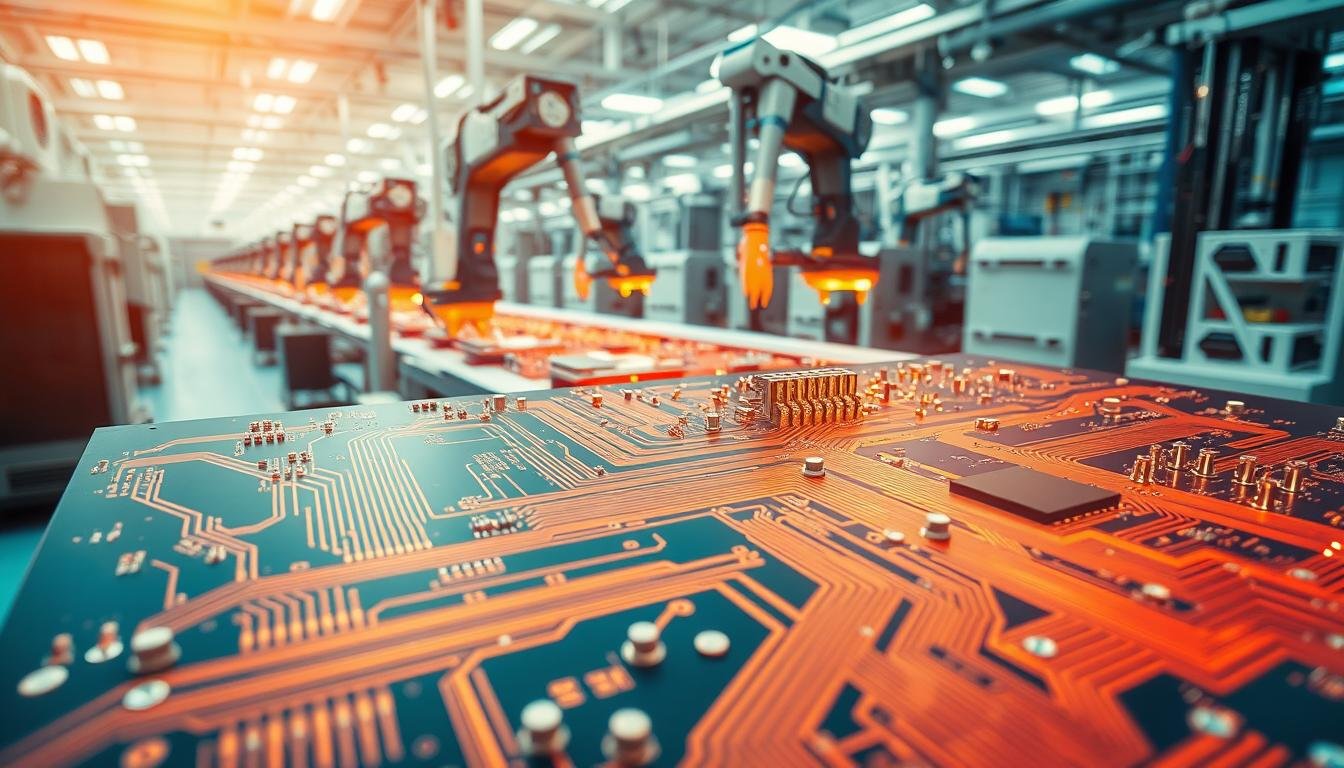
Have you ever wondered what makes a printed circuit board assembly (PCBA) more complicated than it seems? At first glance, a basic PCB appears to be a straightforward component, but the reality is far more complex.
We often encounter clients who are surprised by the intricacies involved in manufacturing what they consider to be a “simple” PCBA. The manufacturing process involves numerous intricate steps that require precision, specialized equipment, and expert knowledge.
Even for boards that appear straightforward at first glance, the design and circuit layout play a crucial role in determining the complexity of the manufacturing process.
Key Takeaways
- Understanding the complexities in PCBA manufacturing helps in planning projects and setting realistic timelines.
- The manufacturing process involves numerous intricate steps requiring precision and expert knowledge.
- Design decisions significantly impact manufacturability, cost, and production timelines.
- Even basic circuit boards require sophisticated processes to create.
- PCBA manufacturing involves more than just mounting components on a non-conductive board.
The Deceptive Simplicity of PCBAs
While PCBAs may appear simple at a glance, their manufacture involves a multitude of complex steps and materials. The foundation of every PCB starts with a base material, typically FR-4, a flame-resistant fiberglass-reinforced epoxy laminate. This base material offers excellent electrical insulation properties while maintaining strong mechanical stability. On top of this foundation, manufacturers apply a thin layer of copper, which will eventually form the conductive pathways essential for the circuit board’s operation.
Common Misconceptions About PCBA Manufacturing
Many assume that because a PCBA looks straightforward, its manufacturing process is simple. However, behind every seemingly simple circuit board lies a complex interplay of materials, processes, and precision engineering that ensures reliable performance in electronic devices. The process involves numerous chemical processes including etching, plating, and application of solder mask—each requiring precise control of temperature, timing, and chemical composition.
- What appears as a straightforward green board with copper traces actually represents multiple layers of specialized materials bonded together with exacting precision.
- Even a basic two-layer PCB requires perfect alignment between layers, precise drilling of holes, and controlled application of surface finishes to ensure proper component attachment and electrical performance.
The Hidden Complexities Behind Every Circuit Board
Understanding these hidden complexities helps explain why PCB manufacturing requires specialized equipment, controlled environments, and expert technicians—even for boards that appear simple in design. We’ve observed that clients are often surprised by the number of quality control steps required throughout the manufacturing process, from automated optical inspection to electrical testing.
| Manufacturing Step | Complexity Involved | Quality Control Measure |
|---|---|---|
| Material Selection | Choosing the right base material and copper thickness | Material inspection |
| Circuit Imaging | Precise application of photoresist and imaging | Automated optical inspection |
| Etching and Plating | Controlled chemical processes for copper layer formation | Chemical composition monitoring |
By understanding the complexities involved in PCBA manufacturing, we can better appreciate the precision and expertise required to produce reliable PCBs for various electronic applications.
The Intricate PCB Manufacturing Process
Creating a PCB requires a series of carefully orchestrated manufacturing steps. The complexity of this process is often underestimated, but it involves multiple stages that demand precision and accuracy to produce a high-quality final product.
From Design to Finished Product: Overview of Manufacturing Steps
The journey from design to a finished PCB involves several critical stages. Initially, the PCB design undergoes a thorough examination to ensure error-free specifications. Engineers rigorously assess the design for potential defects, missing components, or structural difficulties. Any uncaught mistakes at this stage can prove costly later on. The manufacturing process includes various steps such as lamination, etching, and surface finishing, each requiring precise execution.
Critical Precision Requirements at Each Stage
Precision is paramount throughout the PCB manufacturing process. At each stage, from design verification to the final product inspection, maintaining accuracy is crucial. For instance, during lamination, inner layers must be perfectly prepared to avoid defects that become sealed within the board structure. Similarly, surface finishing processes depend on properly prepared copper surfaces, which rely on precise etching and cleaning operations performed earlier in the production sequence.
Why Each Step Builds Upon Previous Ones
The PCB manufacturing process is a chain of interdependent processes where each step depends on the successful completion of previous operations. Errors in early manufacturing stages can compound throughout the process, potentially resulting in costly scrap or rework if not detected and corrected promptly. Understanding this sequential dependency highlights the importance of comprehensive quality control at each stage rather than just inspecting the final product. By ensuring accuracy at every step, manufacturers can avoid cascading issues that affect the final product quality.
We have observed that the interdependence of manufacturing steps is crucial in determining the final quality of the PCB. By acknowledging this interdependence, manufacturers can implement robust quality control measures to mitigate potential issues early on, ensuring a smoother production process and a higher quality final product.
Design Considerations That Impact Manufacturing Complexity
When designing a PCB, several factors can significantly impact the manufacturing complexity. The intricacies of PCB design directly influence the efficiency and cost-effectiveness of the manufacturing process.
Layer Count and Stack-up Challenges
The layer count and stack-up configuration of a PCB are critical design elements that affect manufacturing complexity. As the number of layers increases, so does the difficulty in maintaining precise alignment and avoiding defects. Complex stack-ups can lead to warpage and signal integrity issues, making the manufacturing process more challenging.
| Layer Count | Manufacturing Complexity | Typical Applications |
|---|---|---|
| 2-4 layers | Low-Moderate | Simple electronics, consumer products |
| 6-8 layers | Moderate-High | Complex consumer electronics, industrial controls |
| 10+ layers | High-Very High | Advanced telecommunications, high-performance computing |
Trace Width and Spacing Requirements
Trace width and spacing are crucial for ensuring signal integrity and manufacturability. Tighter tolerances increase the risk of manufacturing defects, such as shorts or opens. Designs with fine traces require advanced manufacturing techniques, including high-resolution photolithography.
Component Density and Placement Constraints
The density and placement of components on a PCB significantly impact manufacturing complexity, particularly during the assembly phase. Components placed too closely together can create challenges for automated pick-and-place equipment, potentially leading to solder bridging or assembly defects.
- Component placement near board edges introduces manufacturing constraints related to panel design and handling.
- Mixed-technology boards combining surface mount and through-hole components require multiple assembly processes, increasing complexity.
- Fine-pitch components demand precise solder paste application and placement accuracy.
By understanding these design considerations, we can create PCBs that are not only electrically functional but also efficient and reliable to manufacture.
Material Selection: More Than Just a Base
Material selection plays a pivotal role in determining the success of a PCB in both design and manufacturing phases. The choice of materials affects not only the circuit board’s performance but also its manufacturability and reliability.
Standard vs. Specialty Materials
When designing a PCB, one of the initial decisions is whether to use standard or specialty materials. Standard materials are typically cost-effective and suitable for most applications, while specialty materials offer unique properties that can be crucial for high-frequency, high-temperature, or high-reliability applications.
Copper Weight and Thickness Considerations
The copper weight and thickness are critical factors in PCB design, directly impacting the board’s electrical performance and thermal management. Thicker copper can handle higher currents but may complicate the manufacturing process.
Surface Finishes and Their Manufacturing Implications
The surface finish of a PCB plays a crucial role in its functionality and longevity. Common finishes include HASL (Hot Air Solder Leveling), ENIG (Electroless Nickel Immersion Gold), Immersion Tin, and Immersion Silver. Each finish offers different benefits for component soldering, environmental protection, and shelf life of the bare boards.
- The selection of surface finish significantly impacts manufacturing processes, assembly yield, and long-term reliability.
- Different finishes require specific manufacturing processes, such as multiple chemical baths for ENIG or specialized equipment for HASL.
- Understanding these considerations helps designers specify appropriate finishes that balance assembly requirements and manufacturing practicality.
Why Your “Simple” PCBA is More Complex to Manufacture Than You Think
While a PCBA may appear simple, its manufacturing process is layered with complexities. The intricacies involved in producing a PCBA are often underestimated, leading to unforeseen challenges and costs. We have encountered numerous instances where seemingly straightforward PCBAs presented significant manufacturing hurdles due to design choices or material specifications.
The Compounding Effect of Design Choices
Design decisions play a crucial role in determining the complexity of PCBA manufacturing. Seemingly minor design choices can have a disproportionate impact on production. For instance, specifying a non-standard PCB thickness for a simple 2-layer board to accommodate a custom connector can complicate the manufacturing process. This may necessitate special material orders or custom lamination, effectively transforming what appeared to be a straightforward project into a more complex one.
- Design decisions that push manufacturing limits in multiple areas simultaneously create compound challenges.
- Specifying non-standard material thicknesses or unusual copper weights can trigger requirements for special material orders.
- The impact of these decisions extends beyond manufacturing to affect testing capabilities and quality control processes.
How Minor Design Decisions Create Major Manufacturing Challenges
Minor design decisions can significantly affect the manufacturability of a PCBA. For example, an unusually small via size or tight tolerance requirement can force the implementation of specialized processes for an otherwise standard board. Understanding how specific design decisions impact manufacturing enables engineers to make informed choices that balance performance requirements with manufacturability.
| Design Aspect | Impact on Manufacturing |
|---|---|
| Non-standard PCB thickness | Requires special material orders or custom lamination |
| Unusually small via size | Necessitates specialized drilling processes |
| Tight tolerance requirements | Demands precise manufacturing and quality control |
By considering the implications of design choices on PCBA manufacturing, we can mitigate unnecessary complexity and optimize production. This proactive approach not only streamlines the manufacturing process but also enhances the overall quality and reliability of the final product.
Manufacturing Bottlenecks You Never Considered

Understanding the intricacies of PCB manufacturing is crucial for efficient production. While designing PCBs, several manufacturing bottlenecks are often overlooked, leading to significant delays and increased costs.
Drilling Challenges: Via Size and Quantity
Drilling is a critical step in PCB production, and via size and quantity can significantly impact manufacturing efficiency. Small vias require precise drilling, and a high quantity can extend production time. “The precision required for drilling small vias can be a significant bottleneck in the manufacturing process,” as it demands advanced machinery and careful process control.
Plating Process Complexities
The plating process is another area where complexities can arise. Ensuring uniform plating thickness, especially in boards with complex geometries or high aspect ratios, can be challenging. This complexity can lead to increased production times and costs if not managed properly.
Routing and Mechanical Processing Limitations
Routing and mechanical processing are critical for defining the outline of PCBs and creating features such as cutouts or cavities. However, these processes have limitations, particularly when it comes to small tools or complex shapes. For instance, using small-diameter routing tools (under 1.5mm) can significantly extend routing cycles because they can only process one panel at a time and operate at reduced speeds to prevent tool breakage.
Complex board outlines with tight-radius corners or intricate shapes require multiple tool changes and reduced routing speeds, further extending production time. Understanding these mechanical processing limitations helps designers create board outlines and mechanical features that balance functional requirements with manufacturing efficiency.
By acknowledging and addressing these manufacturing bottlenecks, designers and manufacturers can work together to optimize the production process, reducing time and costs while improving overall quality.
Tolerance and Specification Challenges
The complexity of PCB manufacturing is often underscored by tolerance and specification challenges that designers must navigate to ensure product viability. In today’s competitive business climate, bringing a project in at a reasonable cost while meeting time-to-market goals is more important than ever.
Designing a product for ease of production will give you your best shot at beating competitors to the punch. A steady and predictable delivery schedule makes it more difficult for similar products to gain a foothold.
The Cost of Tight Tolerances
Tight tolerances in PCB design can significantly drive up production costs. We partner with clients to identify which design features truly require tight tolerances and which can utilize standard specifications without compromising product performance. By doing so, we help reduce unnecessary expenses associated with overly stringent requirements.
Balancing Precision with Manufacturability
The concept of “design for manufacturability” (DFM) represents a systematic approach to balancing precision with production efficiency by considering manufacturing implications during the design phase. Early collaboration between design engineers and manufacturing specialists helps identify potential issues before they become costly problems, allowing for design optimizations that improve both functionality and manufacturability.
Successful PCB design requires finding the optimal balance between precision requirements and manufacturing practicality to create boards that meet functional needs while remaining cost-effective. Understanding this balance helps create designs that not only meet performance requirements but can also be consistently produced with high yield and reasonable cost over time.
Testing and Quality Assurance Complexities

Comprehensive testing is essential to ensure that each PCB functions as intended. Multiple testing methods are employed to verify circuit integrity and component functionality throughout the manufacturing process.
Automated Optical Inspection (AOI) Requirements
Automated Optical Inspection (AOI) is a critical step in the PCB manufacturing process. AOI systems use high-resolution cameras to inspect boards for defects such as shorts, opens, and incorrect component placement. This non-destructive testing method allows for quick identification of issues early in the production cycle, reducing the time and cost associated with rework.
To maximize the effectiveness of AOI, PCBs must be designed with testability in mind. This includes ensuring adequate access for the inspection cameras and designing the circuit layout to facilitate clear visualization of critical components and connections.
Electrical Testing Considerations
Electrical testing represents a crucial quality assurance step that verifies the functional integrity of manufactured PCBs before they enter the assembly process. We implement various testing methodologies, including flying probe, bed-of-nails fixtures, and combinational testing approaches based on board complexity and production volume.
The testability of a PCB design significantly impacts testing efficiency, with factors such as test point accessibility, net isolation, and circuit complexity directly affecting test coverage and cycle time. Understanding these testing-related considerations helps designers create boards with features that facilitate effective electrical verification, potentially improving manufacturing yield and product quality. For more information on the process, visit https://www.wevolver.com/article/test-pcb-everything-you-need-to-know and https://espcba.com/learning-the-pcb-manufacturing-process-from-design-to-production/.
Cost Drivers in PCBA Manufacturing
PCBA manufacturing costs are influenced by a variety of factors, including design and material choices. The complexity of these costs can be broken down into several key areas that significantly impact the final product’s expense.
Non-Standard Features and Their Price Impact
Non-standard features in PCB design can substantially increase manufacturing costs. Features such as unusual board sizes, special materials, or complex circuit designs require specialized processes, leading to higher production expenses. For instance, using high-frequency materials or incorporating blind vias can drive up costs due to the need for advanced manufacturing techniques.
| Non-Standard Feature | Impact on Cost |
|---|---|
| Unusual Board Sizes | Increased material waste and processing complexity |
| Special Materials | Higher material costs and potential supply chain issues |
| Complex Circuit Designs | Increased manufacturing time and potential for errors |
How Early Design Decisions Affect Final Costs
Early design decisions have a significant impact on the final cost of PCBA manufacturing. Choices regarding layer count, component selection, and board size can either optimize or inflate production costs. For example, minimizing layer count and selecting standard components can reduce expenses, while complex designs with dense component placement can increase costs.
By understanding these cost drivers and making informed decisions early in the design process, manufacturers can better control production expenses and deliver cost-effective PCBA solutions.
Conclusion: Designing for Manufacturability
Designing for manufacturability is crucial in ensuring that PCBA designs are both high-performing and efficiently manufactured. By understanding the complexities involved in PCB manufacturing, designers can make informed decisions that balance performance requirements with manufacturing practicality.
We advocate for a collaborative approach where design engineers and manufacturing specialists work together from project inception to optimize both functionality and production efficiency. This approach helps to identify opportunities for leveraging standard PCB processes and materials, reserving non-standard approaches for features that truly require them.
By recognizing that even “simple” circuit boards involve sophisticated manufacturing processes, designers can create more successful products that meet performance goals while maintaining reasonable production costs and timelines. This strategic approach results in products that are both high-performing and efficiently manufactured, ultimately benefiting the end-user and the manufacturer’s bottom line.