When designing a printed circuit board (PCB), several factors come into play to ensure the final product is both functional and reliable. One critical aspect that often goes unnoticed until the manufacturing stage is the aspect ratio of the vias. The aspect ratio, defined as the ratio of the drill depth to the drill diameter, is a fundamental parameter that directly impacts the board’s reliability and manufacturability.
We explore how this ratio affects everything from drilling capabilities to signal integrity, and why it’s essential for engineers and designers to understand its implications. By optimizing the aspect ratio, designers can ensure both performance and manufacturing success.
Key Takeaways
- The aspect ratio is a critical factor in determining PCB reliability.
- Optimizing the aspect ratio is essential for manufacturability.
- A high aspect ratio can lead to manufacturing challenges.
- Understanding the aspect ratio is vital for signal integrity.
- Design decisions are influenced by the aspect ratio.
What is Aspect Ratio in PCB Design?
The aspect ratio in PCB design refers to the ratio of the board’s thickness to the diameter of the smallest drilled hole, typically a via. This ratio is crucial in determining the manufacturability and reliability of a PCB.
Definition and Basic Concept
The aspect ratio is a fundamental concept in PCB design that defines the relationship between the thickness of a PCB and the diameter of its smallest via. Vias are tiny holes that allow electrical connections between different layers of a multi-layer PCB. A higher aspect ratio indicates a thicker board relative to the diameter of the via, which can pose manufacturing challenges.
Mathematical Formula for Aspect Ratio
The formula for calculating the aspect ratio is straightforward: AR = (Board Thickness)/(Hole Diameter). For instance, if a PCB is 1.6mm thick and the smallest via diameter is 0.2mm, the aspect ratio is 8:1. This calculation gives designers a clear metric to work with when assessing manufacturing capabilities and board reliability.
| Board Thickness (mm) | Via Diameter (mm) | Aspect Ratio |
|---|---|---|
| 1.6 | 0.2 | 8:1 |
| 2.4 | 0.3 | 8:1 |
The Importance of Aspect Ratio in PCB Manufacturing
The significance of aspect ratio in PCB manufacturing cannot be overstated, as it directly affects the manufacturability, reliability, and cost implications of PCBs. We recognize that maintaining an optimal aspect ratio is crucial for ensuring the quality and performance of the final product.
Impact on Manufacturability
During the plating process, copper must be deposited uniformly inside the vias to ensure reliable electrical connections. A high aspect ratio (e.g., 10:1 or above) can make it difficult for plating solutions to flow through the narrow holes, leading to uneven copper deposition or voids. This can result in weak connections or complete failures.
Effect on Reliability
Vias with poor plating are prone to cracking or breaking under thermal stress or mechanical strain, especially in high-temperature applications. A balanced aspect ratio helps maintain structural integrity. We emphasize that vias with optimal aspect ratios are less likely to fail, ensuring the overall reliability of the PCB.
Cost Implications
Pushing the limits of aspect ratio (e.g., extremely small vias in thick boards) often requires advanced manufacturing techniques, which can increase production costs. Staying within recommended ratios helps keep expenses in check. We note that manufacturers often specify maximum aspect ratio capabilities based on their equipment and process capabilities.
| Aspect Ratio | Manufacturability | Reliability | Cost |
|---|---|---|---|
| Low (e.g., 5:1) | High | High | Lower |
| High (e.g., 10:1) | Low | Low | Higher |
| Optimal (e.g., 8:1) | Medium | Medium | Moderate |
How to Calculate PCB Aspect Ratio
We calculate the aspect ratio of a PCB by considering the board thickness and the diameter of the smallest drilled hole, a process that is vital for ensuring the quality of the final product.
Step-by-Step Calculation Process
To calculate the aspect ratio, follow these steps:
- Determine the total board thickness, including all copper layers and dielectric materials.
- Identify the diameter of the smallest drilled hole or via in your design.
- Divide the board thickness by the smallest hole diameter to get the aspect ratio.
For instance, if your PCB has a total thickness of 1.6mm and the smallest via diameter is 0.3mm, the aspect ratio would be 1.6mm ÷ 0.3mm = 5.33, or approximately 5.3:1.
Practical Examples
Let’s consider a few practical examples to illustrate the calculation:
- A standard 1.6mm thick PCB with 0.2mm diameter vias would have an aspect ratio of 8:1.
- A 2.4mm thick power electronics board with 0.3mm vias would also have an aspect ratio of 8:1, which is within standard manufacturing capabilities.
- For high-density interconnect (HDI) designs with 1mm thickness and 0.1mm microvias, the aspect ratio would be 10:1, approaching the limits of standard manufacturing processes.
Understanding how to calculate the aspect ratio allows designers to make informed decisions early in the design process, potentially avoiding costly redesigns later.
Optimal Aspect Ratio Values for Different PCB Applications
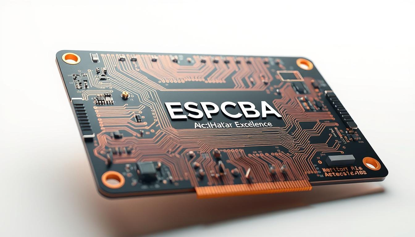
. In the foreground, a ESPCBA branded PCB is displayed, its precise dimensions highlighted by crisp, clean lines. The middle ground features a grid overlay, emphasizing the importance of proportions in PCB design. In the background, a soft, gradient-based environment creates a sense of depth and technical sophistication. Careful lighting from above casts subtle shadows, accentuating the PCB's refined edges and surface details. The overall composition conveys the significance of aspect ratio in achieving high-performance, visually appealing PCB layouts for diverse applications.")
Different PCB applications demand specific aspect ratio considerations based on their unique requirements and constraints. The aspect ratio is a critical factor in determining the manufacturability, reliability, and performance of PCBs.
Standard Consumer Electronics
For most consumer electronics and general-purpose PCBs, an aspect ratio between 6:1 and 8:1 is considered optimal. This translates to via diameters of approximately 0.2mm to 0.27mm for a 1.6mm thick board, ensuring reliable plating and keeping costs low. Aspect ratios within this range balance manufacturability with design density needs. Consumer electronics often utilize boards with via diameters between 0.2mm and 0.27mm, creating aspect ratios that most manufacturers can reliably produce.
High-Density Interconnect (HDI) Designs
In applications requiring high-density interconnects (HDI), such as smartphones or advanced medical devices, aspect ratios may approach 10:1. These designs often use microvias with diameters as small as 0.1mm on thinner boards (e.g., 1mm thick), necessitating advanced manufacturing capabilities. HDI designs push the boundaries of aspect ratios, enabling more components and interconnections in smaller spaces.
Power Electronics and Thick Boards
For thicker boards used in power electronics (e.g., 2.4mm or more), maintaining a lower aspect ratio (around 5:1) is often necessary. This means using larger via diameters (e.g., 0.5mm) to ensure proper plating and thermal management. The layer count of a PCB also influences optimal aspect ratio selection, with higher layer counts often requiring more conservative aspect ratios to ensure manufacturing success.
As we have seen, the optimal aspect ratio varies significantly across different PCB applications. By understanding these requirements, designers and manufacturers can work together to create PCBs that meet the necessary performance, reliability, and cost criteria.
Understanding Aspect Ratio in PCB Design and Manufacturing Challenges
Understanding the challenges associated with aspect ratio is essential for creating reliable and manufacturable PCBs. As we push the boundaries of PCB design, particularly in high-density interconnect (HDI) and high-frequency applications, the aspect ratio becomes a critical factor that can significantly impact both manufacturing and performance.
Drilling Limitations
Drilling small holes with high aspect ratios poses significant challenges. Drill bit breakage and wandering increase significantly when drilling small diameter holes in thicker boards, potentially leading to reliability issues. We have observed that maintaining accuracy during the drilling process is crucial, requiring specialized drill bits and precise equipment.
Plating Issues in High Aspect Ratio Vias
Plating the inside of small, high aspect ratio holes with copper can be difficult, leading to incomplete plating or voids. During the electroplating process, the copper precursor in the plating solution is consumed more quickly in deeper regions of the via, resulting in thinner plating at the center of the via barrel. This non-uniform plating can affect the performance and reliability of the PCB.
Signal Integrity Concerns
High aspect ratio vias can introduce impedance discontinuities and reflections in high-speed signal paths, potentially degrading signal integrity. The capacitive and inductive properties of vias become more pronounced with higher aspect ratios, which can be particularly problematic in high-frequency applications. We must carefully consider these factors when designing PCBs for high-speed applications.
By understanding these challenges, we can better balance design requirements with manufacturing capabilities, ultimately creating more reliable and manufacturable PCBs.
Factors Affecting PCB Aspect Ratio

Several key factors affect the aspect ratio in PCB design, including board thickness, component density, and manufacturing capabilities. Understanding these factors is crucial for achieving optimal PCB performance and manufacturability.
Board Thickness and Layer Count
The aspect ratio of a PCB is primarily influenced by its thickness and layer count. As the layer count increases, the overall board thickness naturally increases, directly impacting the aspect ratio calculation when via diameters remain constant. Thicker boards and higher layer counts typically require more conservative aspect ratios to ensure manufacturability and reliability.
Component Density and Size
The size and density of components on a PCB also impact its aspect ratio. High-density designs with fine-pitch components often require smaller vias to accommodate routing constraints, allowing for higher aspect ratios. In contrast, larger through-hole components necessitate larger vias and holes, which may limit the aspect ratio. Surface mount technology (SMT) components generally enable smaller vias and higher aspect ratios compared to through-hole components.
Manufacturing Process Capabilities
The manufacturing process utilized in making a PCB significantly impacts its aspect ratio. Different manufacturing techniques offer varying capabilities when it comes to creating PCBs with different aspect ratios. Advanced manufacturing processes, such as controlled depth drilling and specialized plating chemistries, can extend aspect ratio capabilities beyond standard limits. For more information on optimizing PCB design, visit our blog on PCB aspect ratio.
By understanding and balancing these factors, designers and manufacturers can work together to create PCBs that meet both performance and manufacturability requirements. As stated by industry experts, “The key to successful PCB design lies in understanding the interplay between design parameters and manufacturing capabilities.”
Advanced Techniques for Managing High Aspect Ratios
Advanced manufacturing techniques have revolutionized the way we manage high aspect ratios in PCB design, enabling more complex and compact electronics. These techniques are crucial for maintaining the reliability and performance of modern PCBs.
Laser Drilling Technology
Laser drilling technology represents a significant advancement in managing high aspect ratios. It allows for the creation of extremely precise, small-diameter holes with minimal drill wandering or damage. We’ve seen laser drilling enable microvias as small as 75μm (3 mils) in diameter, supporting aspect ratios that would be impossible with mechanical drilling alone. This technology minimizes the breaking or wearing of drill bits and reduces errors in the PCB.
Sequential Lamination Processes
Sequential lamination processes build the PCB in stages, allowing for the creation of stacked and staggered via structures that effectively manage high aspect ratio challenges. This build-up approach enables the formation of reliable connections between layers without requiring single vias to span the entire board thickness. As a result, it ensures better adhesion of the copper layers and more precise control of the thickness of each layer.
Staggered and Stacked Via Designs
Staggered via designs distribute connections across multiple layers, reducing the effective aspect ratio of any single via while maintaining the necessary interlayer connectivity. Stacked via structures, where multiple vias are placed directly on top of each other, create reliable connections through high layer count boards without requiring extreme aspect ratios. These designs improve the overall reliability and performance of the PCB.
| Technique | Benefits | Impact on Aspect Ratio |
|---|---|---|
| Laser Drilling | Precise, small-diameter holes; minimal drill wandering | Enables higher aspect ratios |
| Sequential Lamination | Builds PCB in stages; allows for stacked and staggered vias | Reduces effective aspect ratio |
| Staggered and Stacked Vias | Distributes connections across layers; improves reliability | Reduces aspect ratio; improves connectivity |
Industry Standards and Guidelines for Aspect Ratio
The Institute for Printed Circuits (IPC) provides crucial guidelines for aspect ratio in PCB design, serving as a foundational reference for manufacturers and designers alike. These standards are essential for ensuring that PCBs meet both manufacturability and reliability requirements.
IPC Standards for Through-Hole Vias
For through-hole vias, IPC standards specify aspect ratios ranging between 6:1 and 8:1 as standard manufacturing capabilities, with 10:1 representing a more advanced capability. An aspect ratio of 8:1 has become an industry benchmark, balancing design density and manufacturing reliability. According to IPC guidelines, through-hole vias with aspect ratios up to 12:1 are possible but are typically limited to specific applications, such as in 2 mm thick boards with 7 mil drills.
| Via Type | Standard Aspect Ratio | Advanced Aspect Ratio |
|---|---|---|
| Through-Hole Vias | 6:1 to 8:1 | 10:1 |
| Laser-Drilled Microvias | 1:1 | 0.75:1 |
Recommendations for Microvias and HDI Boards
For laser-drilled microvias, IPC-T-50M recommends a maximum aspect ratio of 1:1, though advanced manufacturers can achieve ratios of 0.75:1 with specialized processes. HDI board standards recognize the challenges of microvia structures, providing guidelines for stacked and staggered via designs that manage aspect ratio concerns effectively. These standards help designers create boards with predictable manufacturing outcomes and reliability.
Key Takeaways:
- IPC standards provide essential guidelines for aspect ratio in PCB design.
- Aspect ratios for through-hole vias range from 6:1 to 8:1 for standard manufacturing.
- Laser-drilled microvias should have a maximum aspect ratio of 1:1.
Conclusion: Best Practices for Optimizing Aspect Ratio in Your PCB Designs
Optimizing aspect ratio is crucial for achieving the perfect balance between manufacturability, reliability, and performance in PCB designs. To accomplish this, several best practices should be considered. We recommend starting with conservative aspect ratios (6:1 to 8:1 for through-holes, 0.75:1 for microvias) when designing new boards, especially for critical applications.
Early communication with your PCB manufacturer is essential, as their capabilities may allow for aspect ratios beyond standard guidelines. For high-density designs, leveraging advanced techniques like laser drilling and staggered via structures is more effective than pushing single-via aspect ratios to extremes.
By understanding the fundamental principles of aspect ratio in PCB design and manufacturing, and applying these best practices, you can create boards that balance performance, reliability, and cost-effectiveness. Remember, aspect ratio directly impacts manufacturing yield and cost, making it a critical factor in PCB production.