As we navigate the complexities of electronics manufacturing, a critical question arises: Can your design decisions significantly impact production costs and product quality? The answer lies in embracing Design for Manufacturability (DFM) principles, which have been shown to reduce design time by up to 30% and improve product quality by 15%.
We understand that optimizing your PCB design for your manufacturer’s SMT line is crucial. By implementing DFM guidelines early in the development process, you can prevent costly delays and streamline the transition from prototype to production. Our expertise in electronics manufacturing enables us to guide you through this process, ensuring that your product is designed with manufacturability in mind.
Key Takeaways
- Implementing DFM principles can significantly reduce design time and improve product quality.
- Optimizing PCB design for SMT assembly lines prevents costly delays and streamlines production.
- Collaboration with manufacturers leads to more efficient assembly processes and higher quality products.
- DFM guidelines help in designing products that are easier to manufacture.
- Early adoption of DFM principles is crucial for successful electronics manufacturing projects.
Understanding DFM for Electronics Manufacturing
In the realm of electronics manufacturing, Design for Manufacturability (DFM) stands as a crucial methodology that bridges the gap between design intent and manufacturing reality. As we explore the intricacies of DFM, it becomes clear that this approach is not just beneficial but essential for optimizing product design to facilitate easier, more efficient manufacturing processes.
What is Design for Manufacturability?
Design for Manufacturability is a proactive design approach that anticipates manufacturing challenges before they occur. By optimizing product design, DFM ensures that the product meets the fabricator’s capabilities, including critical parameters such as trace width, drill size, and board edge to copper. This methodology is crucial for minimizing or eliminating board respins, layout changes, and redesigns, ultimately reducing production costs.
DFM serves as a bridge between design intent and manufacturing reality, ensuring that designs are manufacturable and meet quality standards. By implementing DFM rules, manufacturers can significantly reduce the need for costly redesigns and re-validation of board functionalities.
The Business Case for DFM Implementation
The implementation of DFM has a direct and positive impact on the business bottom line. By reducing design iterations, minimizing board respins, and eliminating redesign cycles, DFM implementation leads to significant cost savings. Moreover, DFM enables companies to accelerate their time-to-market while maintaining high-quality standards, thereby creating a competitive advantage in the electronics manufacturing industry.
Our analysis shows that companies that adopt DFM principles early in the design process tend to have lower production costs and faster product deployment. This is because DFM encourages a collaborative approach between designers and manufacturers, ensuring that products are designed with manufacturability in mind from the outset.
| Benefits of DFM | Description | Impact |
|---|---|---|
| Reduced Design Iterations | Fewer changes required during production | Cost Savings |
| Minimized Board Respins | Less need for redesigns | Faster Time-to-Market |
| Improved Quality | Enhanced product reliability | Competitive Advantage |
By embracing DFM, electronics manufacturers can not only reduce costs and improve product quality but also gain a competitive edge in the market. As the industry continues to evolve, the importance of DFM will only continue to grow, making it an essential consideration for any company involved in electronics manufacturing.
Key DFM Principles for PCB Assembly
To ensure efficient PCB assembly, it’s essential to understand the key DFM principles. DFM analysis is a critical process that evaluates the PCB layout to minimize potential problems during manufacturing and assembly. By integrating DFM principles early in the design process, manufacturers can significantly reduce production costs and improve overall product quality.
Cost Reduction Through Early Implementation
Early implementation of DFM analysis in the design process is crucial for identifying potential manufacturing issues before they become costly problems during production. By using CAD tools with properly configured manufacturing constraints, designers can automatically flag potential issues during the design phase. For instance, setting the minimum trace width to 3 mils in the CAD tool will highlight any traces that are less than 3 mils, preventing expensive corrections later in the production cycle.
By adopting DFM principles early on, manufacturers can reduce material waste, minimize assembly errors, and streamline manufacturing processes. This proactive approach not only reduces production costs but also improves the overall efficiency of the manufacturing process.
| DFM Principle | Benefit | Impact on Production |
|---|---|---|
| Early DFM Analysis | Identifies potential manufacturing issues early | Reduces costly corrections during production |
| Proper CAD Tool Configuration | Automatically flags design rule violations | Prevents manufacturing errors |
| Optimized Design for Manufacturability | Reduces material waste and assembly errors | Streamlines manufacturing processes |
Balancing Performance and Manufacturability
While optimizing a design for manufacturing efficiency is crucial, it’s equally important to maintain the performance requirements of the final product. A balanced approach to DFM ensures that the PCB design meets both manufacturability and performance standards. This involves careful consideration of factors such as component placement, spacing, and clearance requirements.
By striking the right balance between manufacturability and performance, manufacturers can produce high-quality PCBs that meet the required specifications while minimizing production costs.
Component Placement Strategies
Effective component placement is crucial for optimizing PCB designs for efficient SMT assembly. Smart component placement is very important for a good prototype.
Optimizing Layout for SMT Assembly
To optimize the layout for SMT assembly, it’s essential to put parts in an order that matches how the board is built. This helps machines work faster and makes fewer mistakes. Using special tools can help you make the best layout, which makes your board work better and last longer.
- Position connectors near the edge so they are easy to reach.
- Avoid placing tall parts next to small ones to prevent shadows when soldering.
- Keep sensitive parts away from things that get hot.
Grouping and Orientation Best Practices
Grouping similar components together and ensuring they face the same direction significantly improves pick-and-place machine efficiency and reduces assembly errors. Proper component orientation is critical for the manufacturability of PCBs.
By following these best practices, you can improve the overall manufacturing yield and ensure that your PCB design is both efficient and reliable.
Spacing and Clearance Requirements
To ensure both the manufacturability and functionality of PCB designs, it’s critical to adhere to specific spacing and clearance guidelines. These requirements are fundamental to preventing manufacturing defects, ensuring electrical safety, and maintaining signal integrity.
Minimum Spacing Guidelines
Minimum spacing between pads, traces, and components is crucial for preventing short circuits and thermal issues. The specific spacing requirements depend on the PCB technology and manufacturing process. For instance, high-voltage applications require greater clearance to prevent arcing, while high-speed designs need adequate spacing to minimize crosstalk.
- Adhere to manufacturer-specific guidelines for minimum spacing to ensure manufacturability.
- Consider the voltage differential and signal frequency when determining spacing requirements.
- Ensure sufficient clearance around components for thermal management and inspection.
Electrical Safety and Signal Integrity Considerations
Adequate spacing and clearance are not only crucial for manufacturability but also for ensuring electrical safety and signal integrity. Proper clearance prevents arcing and maintains insulation integrity, especially in high-voltage applications. Moreover, sufficient spacing between signal traces reduces crosstalk, preserving signal quality in high-speed designs.
By following these guidelines, designers can significantly enhance the reliability and performance of their PCB designs. It’s essential to consult with manufacturers to understand specific requirements and best practices for PCB design manufacturing.
Pad and Via Design Optimization
Optimizing pad and via design is crucial for ensuring the reliability and manufacturability of PCBs. Proper design of these elements directly impacts the quality of solder joints, the efficiency of the manufacturing process, and the overall performance of the PCB.
Pad Dimensions and Shapes
The dimensions and shapes of pads play a critical role in determining the reliability of solder joints. Using normal pad sizes and shapes is recommended for strong solder joints. It’s essential to avoid using pads that are too small or too close together, as this can lead to solder bridging and other defects. Non-Solder Mask Defined (NSMD) pads are typically preferred for most Surface Mount Technology (SMT) parts due to their advantages in solderability and manufacturability.
When designing pads, it’s crucial to consider the specific requirements of different component types. For instance, the pad dimensions for fine-pitch components may need to be adjusted to ensure proper solder coverage without excessive solder bridging. A balanced approach to pad design can significantly enhance manufacturing efficiency and product reliability.
| Pad Type | Advantages | Disadvantages |
|---|---|---|
| NSMD Pads | Improved solderability, better for fine-pitch components | Potential for solder mask misalignment |
| Solder Mask Defined (SMD) Pads | Easier to manufacture, less risk of solder mask misalignment | May not be suitable for fine-pitch components |
Via-in-Pad Considerations and Alternatives
Via-in-pad is a technique used in PCB design where vias are placed directly on the pads of components. While this method can be useful for saving space in densely populated boards, it presents several manufacturing challenges, including the risk of solder flowing away from the joint during reflow. To mitigate this, vias near pads should be covered or filled to prevent solder from escaping.
Alternatives to via-in-pad include using micro-vias or redesigning the PCB layout to accommodate vias in less critical areas. These alternatives can help maintain manufacturing efficiency while ensuring reliable solder joints.
PCB Material Selection and Stack-up Planning

To ensure optimal performance and manufacturability, PCB material selection and stack-up planning are crucial. The choice of materials directly impacts the quality and reliability of the final product, while the stack-up configuration affects both signal integrity and manufacturing efficiency.
Material Properties and Manufacturing Implications
Picking the right materials makes your board strong. Good material choices are the base of PCB DFM guidelines. You must think about how the board handles heat, electricity, and force. Studies show that copper trace width and copper weight change how hot the board gets. For example, wider traces and more copper help keep the board cooler. A 140 mil wide trace with 1 oz./sq. ft. copper carrying 3 A gets about 10°C hotter, while a 40 mil wide trace with 0.5 oz./sq. ft. copper carrying 1 A can get 30°C hotter. Using copper planes or pours can help lower the heat even more.
We provide comprehensive guidance on PCB material selection based on both performance requirements and manufacturing considerations, helping designers make informed decisions that balance functionality with producibility.
Layer Stack-up Strategies for Signal Integrity
Planning the stack-up is a big part of PCB DFM guidelines. Putting signal layers between ground planes helps signals and makes the board work better. Studies show this setup cuts electromagnetic interference by 55%. Layer stack-up planning strategies will be examined in detail, with emphasis on how proper stack-up design significantly improves signal integrity while facilitating more efficient manufacturing.
By understanding the relationship between material properties, copper weight, trace width, and thermal performance, designers can create PCBs that are both manufacturable and reliable. Our guidance will help you make informed decisions that enhance the overall design for manufacturability of your PCB.
Solder Mask and Silkscreen Guidelines
Effective PCB design requires careful consideration of solder mask and silkscreen guidelines to ensure manufacturing reliability and prevent common defects. We will outline critical guidelines that facilitate both assembly and inspection processes, improving overall manufacturing efficiency.
Solder Mask Clearance and Registration
When designing a PCB, it’s essential to watch solder mask clearance to prevent solder bridges and other manufacturing issues. The solder mask keeps copper traces and pads safe from solder bridges. A minimum of 4 mil spacing is recommended between pads for effective solder dams, particularly for green solder masks commonly used in production. Additionally, ensuring proper solder mask registration is crucial to prevent manufacturing issues. We recommend making the solder mask a bit bigger around pads to accommodate any misalignment during the manufacturing process.
Effective Silkscreen Implementation
Silkscreen markings play a vital role in facilitating both assembly and inspection processes. To ensure clarity, we recommend keeping silkscreen text at least 4.5 mil from insulation and 5 mil away from copper pads or traces. The text should be at least 25 mil tall, and lines should be 4 mil wide. These guidelines help prevent silkscreen from covering areas where solder is applied, thus improving manufacturing efficiency.
By following these guidelines for solder mask clearance and silkscreen implementation, designers can significantly enhance the manufacturability and reliability of their PCBs. We emphasize the importance of balancing design considerations with manufacturing requirements to achieve optimal results.
DFM for Assembly: Designing for Your Manufacturer’s SMT Line
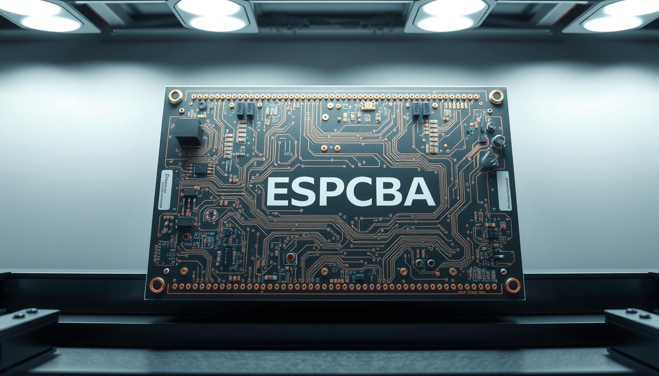
 assembly. The ESPCBA board features a clean, minimalist layout with precisely positioned test points, ensuring seamless integration and troubleshooting on the manufacturer's SMT line. Soft, diffused lighting illuminates the board's surface, highlighting the thoughtful component arrangement and the attention to design for manufacturability. The perspective is slightly elevated, providing a clear overview of the test point distribution across the board, enabling a comprehensive understanding of the DFM principles applied.")
SMT line assembly requires careful consideration of DFM principles to ensure high-quality PCBAs. We will explore how design for manufacturability impacts the assembly process on SMT lines, focusing on critical aspects that improve production efficiency and product reliability.
Test Point Placement and Accessibility
Test points are crucial for ensuring the reliability and testability of PCBs during the manufacturing process. By incorporating test points early in the design phase, you can significantly enhance the manufacturability of your PCB assembly. Strategic placement of test points facilitates automated testing, reducing test time while increasing fault coverage and manufacturing yield.
To maximize the effectiveness of test points, it’s essential to consider their accessibility. We recommend guidelines for test point size, spacing, and location based on common test equipment requirements. Proper test point design enables better connectivity for in-circuit testing (ICT) and functional testing, ultimately leading to faster production and reduced costs.
Component Labeling and Polarity Marking
Clear labels and polarity marks are vital for efficient assembly and to prevent errors during the PCB assembly process. By marking each component’s direction and using silkscreen or laser marks to indicate pin1, plus and minus sides, and part names, you can significantly reduce assembly mistakes.
We provide guidelines for component labeling and polarity marking that align with automated optical inspection (AOI) requirements. Proper implementation of these practices not only prevents assembly errors but also reduces manufacturing defects, ensuring that your PCBs are produced to the highest quality standards.
By focusing on DFM for assembly and incorporating these best practices, you can streamline your manufacturing process, improve product reliability, and reduce production costs. Effective design for manufacturability is key to successful PCB assembly on SMT lines.
Avoiding Common DFM Pitfalls
When designing for manufacturability, it’s crucial to avoid common pitfalls that can lead to production delays and increased costs. We identify and analyze the most common DFM pitfalls that lead to manufacturing problems, providing practical strategies to avoid these costly mistakes in your PCB designs.
Component Orientation Errors
Component orientation errors frequently cause board failures. For instance, improper orientation of diodes, ICs, and LEDs can lead to non-functional assemblies or damaged components. Machines use your design files to know how to place parts. If pin1 or polarity is not marked clearly, mistakes can happen during assembly. To avoid this, we recommend clearly marking component orientation in both design files and silkscreen. Using arrows, dots, or notches can effectively show which way parts go.
Ignoring Manufacturer Specifications
Ignoring manufacturer specifications can also lead to significant issues. Each PCB factory has its own rules for pad sizes, spacing, and materials. If you do not use these specs, you might get soldering problems, weak connections, or even a broken board. We emphasize the critical importance of adhering to manufacturer specifications. By establishing early communication with your manufacturer, you can understand their specific DFM requirements before finalizing designs, preventing expensive revisions and production delays.
By being aware of these common DFM pitfalls and taking steps to avoid them, you can ensure a smoother transition from design to production, reducing costs and improving overall efficiency.
Conclusion: From Prototype to Production
The journey from concept to product requires careful consideration of DFM guidelines to ensure a smooth transition to high-volume production. Throughout this article, we’ve explored key design for manufacturability principles that significantly impact the efficiency and quality of electronics manufacturing. By implementing these DFM practices early in the design process, companies can reduce design iterations, minimize manufacturing defects, and accelerate time-to-market for new products.
Partnering with a reliable PCB assembly factory can further enhance production efficiency. Effective DFM implementation not only improves product quality but also provides a competitive advantage in the fast-paced electronics industry. To achieve this, we recommend integrating DFM thinking into your organizational culture, making manufacturability considerations a natural part of the design process. For more information on optimizing your PCB design for production, visit PCB prototype services that can help streamline your manufacturing workflow.
By establishing strong design-manufacturing collaboration, electronics companies can continue to deliver value throughout the product lifecycle management, ultimately enhancing their bottom line. As the electronics manufacturing landscape continues to evolve, embracing DFM principles will be crucial for staying competitive.