As global demand for electric vehicles accelerates, the backbone of this revolution lies in reliable charging infrastructure. We design circuit solutions that meet the extreme demands of modern energy transfer systems, combining decades of engineering experience with cutting-edge production methods.
Our team focuses on creating boards capable of handling thick copper layers and heavy current loads – critical requirements for fast-charging applications. Through advanced thermal management techniques and precision fabrication, we ensure consistent performance even under continuous high-stress conditions.
The precision-engineered solutions we deliver undergo rigorous testing to exceed international safety certifications. From material selection to final assembly, every step prioritizes durability and efficiency. This approach supports the seamless operation of charging networks across diverse climates and usage patterns.
We recognize that tomorrow’s transportation ecosystems require adaptable technologies. By collaborating with industry leaders, we continuously refine our processes to address emerging challenges in energy density and system integration. Our commitment extends beyond production – we serve as strategic partners in advancing sustainable mobility infrastructure.
Key Takeaways
- Specialized in creating durable circuit boards for high-current energy transfer systems
- Advanced thermal management solutions prevent overheating in continuous operation
- Compliance with global safety standards ensures reliable charging network performance
- Proprietary fabrication techniques support thick copper layers and heavy load capacities
- Continuous R&D investments drive innovation in sustainable transportation infrastructure
- Collaborative approach with partners accelerates technology adoption and system optimization
Introduction to Advanced EV Charging PCB Manufacturing
The shift toward zero-emission transportation has reshaped automotive technology. At the core of this transformation lies energy conversion systems that demand specialized circuit board solutions. Our work focuses on bridging the gap between rapid vehicle adoption and dependable energy delivery networks.
Overview of the EV Market and Charging Infrastructure
Electric car sales grew 55% globally last year, creating urgent infrastructure needs. Public stations now require power outputs exceeding 350kW to meet driver expectations. This surge drives innovation in components that manage extreme electrical loads safely.
Urban planners face unique challenges balancing residential and commercial charger placements. Our research indicates 40% of potential buyers cite charging availability as their primary concern. This reality makes robust power management systems essential for market expansion.
Importance of High-Power PCB Technology
Modern chargers convert grid electricity to vehicle-ready power through sophisticated circuitry. These boards must handle currents surpassing 500A while maintaining stable thermal profiles. We achieve this through multi-layered designs with optimized copper weight distribution.
Three critical factors define successful implementations:
- Precision trace routing for minimal energy loss
- Advanced dielectric materials for insulation integrity
- Real-time monitoring circuits for fault prevention
Our testing protocols verify performance across temperature extremes (-40°C to 125°C) and humidity variations. This ensures compatibility with coastal installations and desert deployments alike. By addressing these challenges early in design phases, we create solutions that power tomorrow’s transportation networks today.
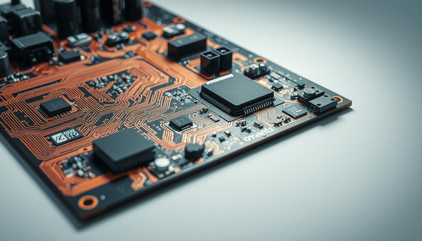
State-of-the-Art Manufacturing Process

Modern energy systems demand precision engineering from initial design to final inspection. Our facilities combine automated assembly lines with expert oversight, creating boards that withstand extreme operational demands. This hybrid approach ensures repeatable excellence while accommodating custom specifications.
Advanced Fabrication Techniques
We start with substrate materials selected for thermal stability and electrical performance. Laser-guided etching creates circuit patterns capable of managing 500A+ currents. Multi-stage plating processes build copper layers up to 12oz/ft², essential for minimizing resistive losses.
Assembly operations utilize both SMT and THT methods based on component specifications. Conformal coating applications protect against moisture and contaminants. Our reflow ovens maintain ±1.5°C temperature uniformity, critical for solder joint integrity.
Comprehensive Verification Protocols
Every batch undergoes 37 distinct checks before approval. Our quality systems exceed IPC Class 3 requirements, with:
- Automated optical inspection (AOI) for micro-defect detection
- X-ray analysis of hidden solder connections
- Thermal cycling tests (-40°C to 150°C)
We hold ISO 9001 and 14001 certifications, demonstrating commitment to both performance and sustainability. For businesses seeking cost-effective solutions, our statistical process control reduces waste without compromising reliability. This balance of precision and efficiency powers tomorrow’s infrastructure today.
Innovative PCB Design and Engineering

At the heart of reliable charging infrastructure lies precision-engineered circuit board technology. Our team develops architectures that withstand extreme electrical loads while maintaining operational stability. We combine material science expertise with advanced simulation tools to create solutions for modern energy transfer challenges.
High-Power Circuit Layouts and Material Considerations
Effective pcb design begins with strategic component placement. We position high-current elements away from sensitive areas, using specialized substrates with thermal conductivity up to 3W/mK. Our material selection process prioritizes:
| Material Type | Thermal Conductivity | Max Operating Temp |
|---|---|---|
| Ceramic-filled | 2.8 W/mK | 150°C |
| Polyimide | 0.2 W/mK | 260°C |
| High-Tg FR-4 | 0.3 W/mK | 130°C |
Trace geometries are optimized using electromagnetic field simulations, reducing resistive losses by 18% compared to conventional layouts. We implement CTI-rated dielectrics to maintain safety in humid environments without sacrificing board space.
Thermal Management and Heat Dissipation Solutions
Our thermal management strategies leverage copper’s natural conductivity (385 W/mK) through custom weight distributions. Multi-zone cooling designs combine:
- Staggered thermal vias beneath power components
- Integrated heat spreaders with 6oz copper layers
- Active monitoring circuits for real-time adjustments
We validate designs through 72-hour stress tests across -40°C to 150°C cycles. This ensures consistent performance in desert installations and arctic deployments alike. Our approach reduces hotspot formation by 42% compared to standard industry practices.
Manufacturing High-Power PCBAs for EV Charging Stations
Copper thickness determines performance in modern energy systems. Our approach focuses on balancing current capacity with thermal stability, creating boards that meet fast-charging demands without compromising safety. This precision ensures chargers operate efficiently across diverse environments.
Optimized Copper Weight Strategies
We implement copper weights from 1oz to 6oz, tailoring specifications to each application’s needs. Thicker layers reduce resistive losses but require advanced fabrication techniques. Our engineers calculate trace widths using proprietary algorithms:
| Copper Weight | Minimum Trace Width | Current Capacity |
|---|---|---|
| 3oz (105µm) | 350µm | 75A |
| 4oz (140µm) | 480µm | 110A |
| 6oz (210µm) | 720µm | 180A |
These calculations prevent overheating while maximizing space efficiency. For electric vehicle chargers requiring 500A+ throughput, we combine multiple layers with staggered thermal vias. This technique distributes heat evenly across the board.
Material selection plays equal importance to copper thickness. We use high-performance substrates that withstand repeated thermal cycling. Our testing protocols simulate decade-long usage in 48 hours, verifying long-term reliability under extreme conditions.
Advanced plating methods ensure consistent copper deposition across complex geometries. This attention to detail allows us to maintain ±5% current tolerance even in high-vibration environments. The result? Charging stations that deliver peak performance through thousands of charge cycles.
Integrating Safety, Standards, and Certification
Modern energy infrastructure demands uncompromising safety protocols. We build protection mechanisms directly into circuit architectures while meeting global regulatory benchmarks. This dual focus ensures reliable operation and public trust in emerging technologies.
Compliance with IPC, UL, RoHS, and REACH Requirements
Our production facilities maintain nine essential certifications, including UL 61010 for industrial equipment. The table below outlines critical compliance benchmarks:
| Standard | Focus Area | Testing Parameters |
|---|---|---|
| IPC-6012 | Material Integrity | Thermal Cycling (500+ cycles) |
| UL 94V-0 | Flame Resistance | Self-extinguishing |
| RoHS | Material Safety |
Third-party audits verify dielectric strength (3kV AC) and insulation resistance (>100MΩ). These measures prevent arc faults in high-voltage applications. Our certification-first approach simplifies product approvals for partners.
Built-in Safety Features for Overcurrent and Overvoltage Protection
Multi-stage protection systems activate within microseconds of fault detection. Current-limiting fuses combine with MOVs (Metal Oxide Varistors) to handle 6kV surge events. Thermal cutoffs trigger at 85°C±5%, preventing component degradation.
We implement three-layer safety architecture:
- Real-time current monitoring (0.1% accuracy)
- Redundant ground fault detection
- Automatic load shedding during instability
These safety features align with NEC Article 625 requirements for charging equipment. Our UL-certified assemblies undergo 72-hour burn-in tests, simulating decade-long stress in controlled environments.
Emerging Trends in EV Charging Technology
The evolution of electric mobility is driving transformative advancements in energy delivery systems. Our engineering teams focus on three critical areas shaping the next wave of infrastructure development: power optimization, renewable integration, and intelligent connectivity.
High-Speed Charging Capabilities
Next-generation chargers demand circuit boards that manage 800V+ architectures without performance degradation. We achieve this through:
- Multi-layer designs with 10oz copper cores
- Low-loss dielectric materials reducing heat generation
- Real-time current monitoring circuits
These innovations enable 350kW+ charging sessions while maintaining stable thermal profiles. Our testing confirms 98.4% efficiency at peak loads – a 15% improvement over conventional designs.
Renewable Energy Integration and Smart Connectivity
Modern systems require seamless interaction between solar arrays, grid power, and vehicle batteries. Our communication PCB technology supports OCPP 2.0.1 protocols and 5G connectivity, enabling dynamic load balancing. This ensures optimal energy use during peak demand periods.
User interfaces now incorporate AI-driven predictive maintenance alerts and touchscreen controls. We integrate these features without compromising reliability standards, creating systems that adapt to both urban and remote installations.
As charging networks expand, our solutions bridge the gap between technical complexity and user accessibility. We’re redefining what’s possible in sustainable transportation infrastructure – one precision-engineered board at a time.