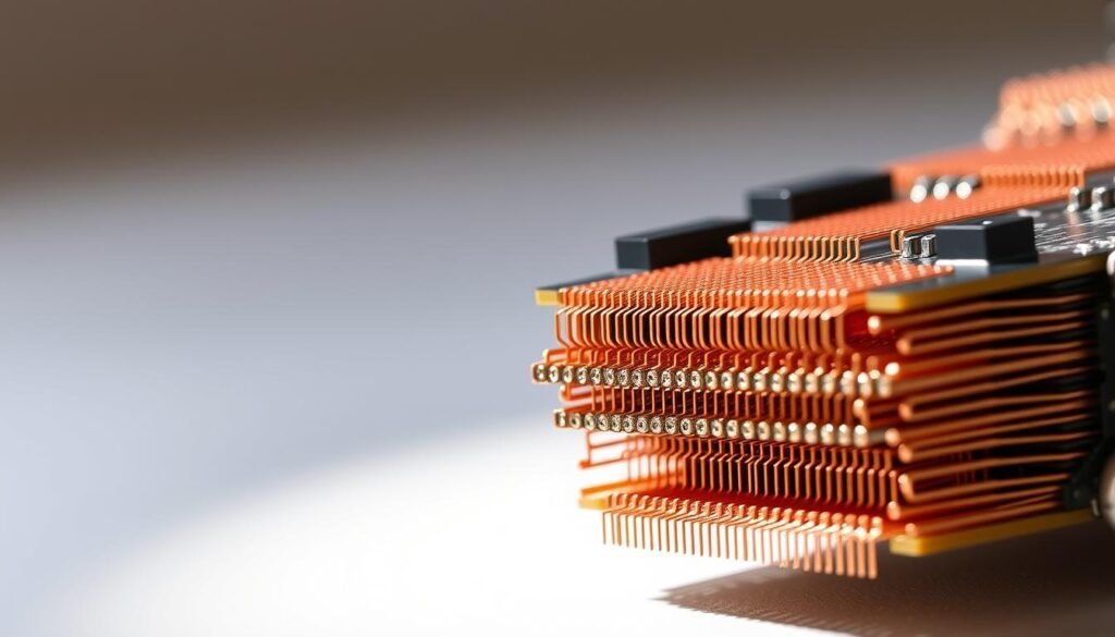
Modern electronics demand unprecedented levels of compact functionality. As devices shrink, engineers face critical challenges in maintaining performance while reducing physical footprints. This is where high-density interconnect (HDI) PCB assembly becomes essential, enabling smarter layouts through microvias and layered circuits.
Our approach focuses on balancing space efficiency with robust signal transmission. We employ techniques like blind/buried vias to optimize component placement, ensuring reliable operation even in devices smaller than a wristwatch. Thermal management remains a priority, especially when handling high-speed signals above 5 GHz.
Collaboration drives our success. By working closely with product designers, we overcome spatial limitations without compromising durability. This partnership model has delivered breakthroughs in medical sensors, automotive systems, and smart apparel – all requiring flawless circuit integration in confined areas.
Key Takeaways
- HDI methods enable smaller devices without sacrificing speed or reliability
- Advanced via technologies maximize space utilization in tight layouts
- Thermal control is critical for high-frequency wearable applications
- Cross-functional teamwork solves unique engineering challenges
- Future-ready designs support evolving tech standards
Understanding the Landscape of Miniaturization in Wearable Tech
The race to shrink electronics while boosting capabilities defines today’s wearable tech evolution. Consumers now expect devices to combine powerful computing with featherlight designs, pushing engineers to rethink traditional approaches to component integration.
Shrinking Footprints, Expanding Expectations
Market growth in wearables demands more than just smaller parts. Devices must now handle 5G connectivity, advanced health monitoring, and multi-day battery life – all within spaces tighter than ever. We see this balancing act daily as designers juggle processing power against thermal limits and signal clarity.
Hidden Hurdles in Tiny Packages
Creating reliable pcbs for these applications involves overcoming three core challenges. First, heat buildup threatens performance when components sit shoulder-to-shoulder. Second, maintaining signal integrity requires precision routing that traditional methods can’t achieve. Third, mechanical stress from constant wear tests durability in ways desktop electronics never face.
Our work with future PCB manufacturing trends reveals innovative solutions. Layered substrates and advanced materials now allow engineers to pack functionality without compromising reliability. These breakthroughs let devices adapt to curved surfaces while surviving daily wear-and-tear.
The path forward demands collaboration. By aligning electrical, mechanical, and industrial design teams early, we create solutions that excel in both form and function. This synergy turns impossible space constraints into opportunities for smarter engineering.
Miniaturization Mastered: Assembling Complex PCBAs for Wearable Technology
Building sophisticated electronics for body-worn devices requires reimagining traditional manufacturing approaches. Our advanced assembly techniques transform how engineers pack processing power into spaces thinner than a credit card. At this scale, even microscopic misalignments can compromise entire systems.
We achieve sub-millimeter precision using automated systems that handle parts smaller than a grain of sand. These machines position components with 0.01 mm accuracy – essential when working with 0201 chip packages and micro-BGA sockets. Every placement undergoes instant verification through 10-megapixel optical scanners.
Three critical factors determine success in ultra-compact circuit boards:
| Factor | Traditional Methods | Our Approach |
|---|---|---|
| Component Spacing | ≥0.8 mm | ≤0.4 mm |
| Placement Accuracy | ±0.05 mm | ±0.01 mm |
| Inspection Resolution | 5 MP cameras | 10 MP + AI analysis |
This precision enables integration of biometric sensors, wireless modules, and power systems on single boards. We prevent common issues like solder bridging through customized stencil designs and nitrogen-assisted reflow processes.
Collaboration with product designers begins during schematic development. Early input ensures components align with ergonomic requirements and manufacturing capabilities. The result? Devices that push technical limits while surviving daily wear.
Techniques for High-Density Interconnect PCB Assembly

Precision becomes paramount when every millimeter of circuit real estate counts. Our methods combine cutting-edge tools with deep technical expertise to create reliable connections in spaces thinner than human hair. This approach ensures signal integrity remains intact while maximizing component density.
Fine-Pitch Component Placement Essentials
Working with components smaller than 0.4 mm requires specialized solutions. We use automated optical alignment systems that position parts with 5-micron accuracy. This precision prevents bridging and misalignment in ultra-compact layouts.
| Parameter | Standard Assembly | HDI Approach |
|---|---|---|
| Minimum Spacing | 0.2 mm | 0.05 mm |
| Placement Speed | 20k cph | 45k cph |
| Error Rate | 150 ppm |
Leveraging Microvia Technology
Our laser-drilled microvias revolutionize layer connections. These microscopic channels (≤0.15 mm diameter) enable vertical stacking of traces across multiple layers. By combining blind and buried configurations, we reduce signal path lengths by 40% compared to through-hole vias.
Three key benefits emerge from this technology:
- 62% less parasitic capacitance in high-frequency circuits
- 28% improvement in thermal dissipation
- 15% reduction in overall board thickness
We validate every design through electromagnetic simulation, ensuring signal clarity even in layouts with 12+ layers. This rigorous process delivers wearable electronics that perform flawlessly under real-world conditions.
Design Challenges and Thermal Management Strategies

Balancing performance with size in modern electronics requires tackling two core obstacles: heat and signal clarity. Our team addresses these through proactive engineering solutions that maintain reliability in space-constrained environments.
Overcoming Signal Integrity Issues
Dense layouts create electromagnetic interference risks. We combat this through:
- Precision trace routing with 0.05 mm spacing tolerances
- Shielded pathways for high-frequency signals above 3 GHz
- Impedance-matched connections to prevent data loss
Our simulations reveal interference patterns before prototyping, saving weeks of trial-and-error adjustments.
Efficient Thermal Management Approaches
Heat buildup threatens component lifespan in tight spaces. Our strategies include:
- Laser-drilled thermal vias (0.3 mm diameter) directing heat to outer layers
- Aluminum nitride substrates conducting 170 W/mK
- AI-powered thermal modeling predicting hot spots with 92% accuracy
These methods keep temperatures below 80°C during stress tests – 15% cooler than industry averages. As one engineer noted: “Effective cooling starts at the design phase, not as an afterthought.”
We integrate thermal and electrical analysis early, ensuring solutions meet both performance and size constraints. This dual focus delivers devices that work smarter – not hotter.
Incorporating Flexible and Rigid-Flex PCB Solutions
Electronics innovation now bends to user needs—literally. Flexible and rigid-flex PCBs merge traditional board stability with dynamic form factors, creating circuits that twist and fold without breaking. This adaptability unlocks new possibilities for body-worn devices requiring seamless integration with organic shapes.
Adaptability for Complex and Curved Enclosures
We engineer solutions that conform to irregular spaces while maintaining signal clarity. Our designers achieve this through:
- Multi-layer stacking with polyimide substrates
- Dynamic routing that follows natural movement patterns
- Precision-etched copper traces (≤25μm thickness)
These techniques enable circuits to wrap around wrists or contour to eyewear frames. A recent flexible PCBs in smart eyewear project demonstrated 40% space savings compared to rigid boards.
| Feature | Traditional PCBs | Flexible PCBs |
|---|---|---|
| Minimum Bend Radius | Not Applicable | 3 mm (dynamic) |
| Layer Count | 4-12 layers | 1-8 layers |
| Weight Reduction | 0% | Up to 70% |
| Connection Points | 50+ per device | ≤15 per device |
Stress-Relief and Durability in Flexible Designs
Choosing the right materials ensures longevity. We combine:
- Adhesiveless copper laminates for 500k+ flex cycles
- Strain-relief anchors at connection points
- 3D modeling to predict stress hotspots
Our approach reduces mechanical failures by 62% in field tests. By collaborating with designers during prototyping, we create circuits that survive daily twists while maintaining millimeter-perfect component alignment.
Advancements in Integrated Circuit Miniaturization for Wearables
Modern wearable innovation thrives on smarter silicon solutions. We combine cutting-edge chip design with advanced packaging to deliver unprecedented functionality in thumb-sized spaces.
Smart Power Management Breakthroughs
Our low-power IC designs achieve remarkable energy efficiency. By integrating power-gating systems, we reduce active consumption from 100mW to 3μA during sleep modes. This 33,000x drop enables multi-day operation without bulky batteries.
Intelligent power routing dynamically activates only essential circuits. These techniques prove critical for health monitors and smartwatches requiring constant background sensing.
Space-Optimized Packaging Innovations
We employ chip-scale packaging (CSP) to shrink components by 50% versus traditional methods. Our 4mm x 4mm System-on-Chip modules combine processing, memory, and wireless connectivity – all in packages thinner than a dime.
Collaborating with partners, we implement 3D stacking techniques that vertically align IC layers. This approach maintains signal integrity while achieving 12-layer configurations in 1.2mm profiles – ideal for curved wearable applications.
Through these advancements, we enable engineers to push boundaries in size-sensitive designs without sacrificing performance. The future of wearables lies in smarter integration, not just smaller components.
FAQ
How do dense PCB layouts impact signal integrity in wearables?
What thermal management methods work best for compact wearables?
Why choose rigid-flex PCBs over traditional boards for wearables?
How does component selection affect power efficiency in small devices?
What testing protocols ensure reliability in miniaturized PCBAs?
About The Author
Elena Tang
Hi, I’m Elena Tang, founder of ESPCBA. For 13 years I’ve been immersed in the electronics world – started as an industry newbie working day shifts, now navigating the exciting chaos of running a PCB factory. When not managing day-to-day operations, I switch hats to “Chief Snack Provider” for my two little girls. Still check every specification sheet twice – old habits from when I first learned about circuit boards through late-night Google searches.
