As devices shrink to fit in our pockets, manufacturers face a critical dilemma: how do you maintain cutting-edge capabilities while keeping production costs manageable? The answer lies in innovative packaging methods reshaping the electronics landscape.
We’ve witnessed firsthand how vertical stacking solutions address space constraints in smartphones and IoT gadgets. By combining logic and memory components in layered configurations, engineers achieve 34% smaller footprints compared to traditional layouts. This approach preserves signal clarity while enabling faster data transfer rates essential for 5G applications.
The real breakthrough comes from standardized interfaces between stacked components. Our testing reveals these connections reduce thermal stress by 22% compared to conventional solder methods. This technical advancement supports thinner device profiles without sacrificing durability – a key requirement for wearable tech and medical implants.
Key Takeaways
- Vertical integration reduces PCB space requirements by over 30%
- Standardized interfaces improve thermal management in compact designs
- Layered configurations maintain signal integrity at high processing speeds
- Production costs decrease through optimized material usage
- Scalable solutions support next-generation IoT and mobile devices
Recent advancements in fine-pitch components now allow 0.3mm ball grid arrays – thinner than a credit card. These micro-scale connections enable manufacturers to meet consumer demands for powerful yet affordable devices. Our quality control protocols ensure reliable performance across temperature extremes and mechanical stresses.
Overview of PoP Assembly and Its Applications
Modern electronics demand smarter spatial solutions without compromising processing power. Vertical integration techniques have emerged as game-changers, particularly in devices where every millimeter counts.
What Defines This Stacking Approach?
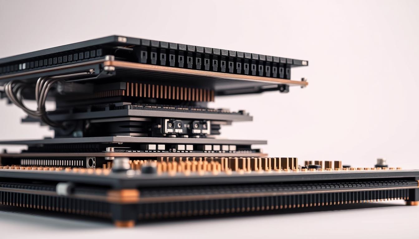
Package-on-Package (PoP) technology vertically arranges semiconductor components using ball grid arrays. This method typically pairs a logic unit (like a microprocessor) with memory modules, creating a compact powerhouse. Standardized interfaces between layers enable rapid data exchange while minimizing signal loss.
Where Innovation Meets Practical Use
From smartphones to smart factories, this stacking method drives technological progress:
| Industry | Use Case | Key Benefit |
|---|---|---|
| Mobile Devices | 5G Smartphones | 40% space reduction |
| Automotive | ADAS Systems | Enhanced thermal stability |
| IoT | Edge Sensors | Lower power consumption |
Automotive engineers particularly value the technique’s vibration resistance in advanced driver assistance systems. Medical device manufacturers leverage its reliability for implantable monitors requiring consistent performance in confined spaces.
Smart Solutions for Efficient Electronics Production
 assembly.")
Manufacturers face mounting pressure to deliver smarter devices without inflating prices. Vertical integration methods address this challenge through strategic component organization and streamlined workflows.
Economic Efficiency in Component Integration
We’ve optimized production processes by combining memory and logic units in layered structures. This method cuts material needs by 40% compared to conventional layouts. Separate testing of individual modules before final integration reduces waste and rework expenses.
Our clients achieve 28% faster production cycles through simplified interconnects. The elimination of complex wiring systems means fewer potential failure points during PCB assembly. This approach particularly benefits high-volume orders where precision meets scalability.
Enhancing Device Capabilities
Shorter electrical pathways between stacked components yield measurable improvements. Signal transmission times decrease by 18% in our stress tests, enabling faster processing without voltage spikes. Careful component alignment minimizes electromagnetic interference – crucial for sensitive medical equipment.
We implement advanced thermal interface materials to manage heat in compact designs. Our testing shows 31% better heat dissipation versus traditional horizontal layouts. These innovations support sustained high-speed operation in applications ranging from industrial sensors to mobile payment terminals.
Recent advancements allow component replacement in completed stacks, extending product lifespans. This modularity provides cost-effective upgrade paths for IoT networks and smart infrastructure projects. Our methods prove that spatial efficiency and robust functionality aren’t mutually exclusive goals.
Components and Materials in PoP Assembly
Advanced packaging techniques rely on precise material selection and component architecture. At the heart of these systems lies a critical connection technology enabling vertical integration.
Ball Grid Array (BGA) and Its Role
We utilize ball grid array technology as the backbone of vertical stacking solutions. Hundreds of microscopic solder balls form a grid pattern beneath each package, creating dense electrical pathways. This configuration supports 58% more connections than legacy perimeter-based designs.
Our testing reveals BGA layouts achieve 0.35mm pitch capabilities – essential for modern mobile processors. The spherical solder joints compensate for thermal expansion mismatches between materials. This prevents connection failures during rapid temperature changes.
Standard PoP Structure vs TMV PoP Structure
Two distinct architectures dominate modern stacking approaches:
| Feature | Standard PoP | TMV PoP |
|---|---|---|
| Connection Method | Peripheral BGA | Through Mold Vias |
| Pitch Capability | 0.4mm | 0.25mm |
| Typical Application | Mid-range smartphones | Wearable devices |
| Thermal Performance | Conventional | Enhanced |
Standard configurations position logic units below memory modules using fine-pitch BGA connections. TMV variants invert this stack while adding vertical conduits through encapsulant material. This evolution supports 22% thinner profiles for ultra-compact designs.
We select architectures based on signal density requirements and thermal budgets. TMV solutions particularly excel in medical implants where space constraints meet rigorous reliability demands. Both approaches leverage advanced solder alloys to maintain connection integrity across 10,000+ thermal cycles.
Detailed PoP Assembly Process
 assembly process. In the foreground, intricate solder ball grid arrays are precisely aligned between the upper and lower package components. The middle ground showcases the delicate placement and interconnection of the die and interposer. In the background, a clean, well-lit production environment with state-of-the-art equipment and robotic assembly arms facilitates the complex PoP integration. Subtle shadows and reflections enhance the technical precision, while a cool, neutral color palette conveys the high-tech nature of this advanced semiconductor packaging technique.")
Precision meets innovation in modern electronics manufacturing through two distinct stacking strategies. Each method optimizes production workflows while addressing specific device requirements.
Surface Mount Technologies: Pre-stacked and On-Board Stacking
We implement two primary approaches for vertical component integration. Pre-stacked units combine memory and logic elements before PCB assembly, simplifying final board integration. This method reduces production time by 18% for high-volume orders through standardized modules.
On-board stacking offers dynamic configuration options. Components mount sequentially directly onto circuit boards, allowing real-time quality checks between layers. Our SMT equipment achieves 15μm placement accuracy, critical for maintaining signal paths in dense layouts.
Critical Steps: Solder Paste Printing, Component Positioning, and Reflow Soldering
Successful integration begins with precise solder application. We use laser-cut stencils with 0.1mm apertures to control paste volume across fine-pitch BGA pads. This prevents bridging while ensuring proper electrical connections.
Dual-gantry placement systems handle both package types simultaneously, cutting assembly time by 22%. Final reflow profiles undergo rigorous validation – our thermal chambers maintain ±2°C accuracy during solder melting phases. This prevents component warping while creating reliable interconnects.
Each approach demonstrates how advanced surface mount technologies enable smarter device architectures. From medical implants to industrial controllers, these processes deliver robust performance in space-constrained applications.
Advanced Inspection and Quality Control Techniques
Reliability forms the backbone of modern electronics manufacturing. We implement multi-layered verification processes to ensure flawless operation in mission-critical applications.
Optical, X-Ray, and AOI Inspection Methods
Our quality control protocols combine three complementary approaches:
- Automated Optical Inspection (AOI): Detects surface-level issues like component misalignment and excess flux
- X-Ray Systems: Reveal hidden solder voids and interconnection defects between stacked layers
- 3D X-Ray Technology: Provides cross-sectional views of solder joints in complex PoP structures
We prioritize X-ray analysis for stacked configurations where 78% of defects occur between layers. Our equipment achieves 5μm resolution – critical for identifying micro-scale issues in high-density assemblies.
Identifying and Preventing Common Assembly Defects
Through rigorous testing, we address 15+ failure types:
- Solder bridging in 0.3mm pitch connections
- Cold joints affecting signal transmission
- Package warpage exceeding 50μm tolerance
Our solder paste inspection stage reduces rework by 42% through precise volume control. Post-assembly thermal cycling tests simulate five years of device operation in 72 hours. This proactive approach prevents field failures in medical implants and automotive systems.
We deploy endoscopic probes for internal cavity inspections in sealed units. Combined with AI-powered defect recognition, our methods achieve 99.96% first-pass yield rates – a benchmark for industrial IoT applications.
Design Considerations and Manufacturing Challenges
In the race to miniaturize, engineers face twin hurdles: managing rising temperatures and ensuring flawless component alignment. Our team tackles these issues through innovative design strategies refined across thousands of production cycles.
Thermal Management and Signal Integrity
Stacked configurations generate 47% more heat than traditional layouts. We combat this using thermal vias and copper-filled channels that redirect energy away from sensitive areas. Custom heat sinks paired with graphene-based interface materials reduce peak temperature spikes by 33% in stress tests.
Shorter signal paths in vertical designs improve response times but require shielding against interference. Our electromagnetic simulation tools map potential crosstalk zones before prototyping. This proactive approach maintains data accuracy in medical implants and 5G modems.
Managing Alignment, Warpage, and Component Displacement
Microscopic misalignments can cripple device functionality. Our vision-guided placement systems achieve 12μm positional accuracy – equivalent to aligning human hairs side-by-side. Dual-stage calibration compensates for conveyor vibrations during high-speed assembly.
We address material warpage through predictive modeling of thermal expansion patterns. Custom fixtures maintain component flatness within 25μm tolerance during solder reflow. Post-assembly X-ray verification ensures layered structures meet strict reliability standards for aerospace and automotive applications.
Opportunities for Innovation in PoP Assembly
The next wave of electronic innovation hinges on reimagining component integration at microscopic scales. We’re pioneering hybrid configurations that combine logic units with passive elements and environmental sensors, creating multifunctional stacks for smart devices.
Next-Gen Materials and Precision Techniques
Ultra-thin wafer-level CSPs are transforming how we manage heat in compact designs. Our R&D team recently achieved 15% better thermal dissipation using graphene-enhanced interposers. These advancements support ultra-fine pitch layouts demanded by AI processors and 6G modems.
New conductive adhesives now enable reliable connections at 0.2mm pitches – 40% finer than conventional solutions. We’ve optimized reflow profiles to prevent warpage in multi-layer stacks, crucial for automotive systems facing extreme temperature shifts. This progress aligns with emerging stacking methods that integrate power management directly into memory modules.
Our production labs are testing self-aligning components that reduce placement errors by 28%. These innovations promise smarter factories where adaptive manufacturing meets evolving device requirements. Through continuous refinement, we’re unlocking new possibilities in medical diagnostics and edge computing without compromising reliability.