Modern electronics demand more than basic power delivery. While most users focus on wall adapters, the real magic happens in the charging modules that manage energy flow. From smartphones to wearables, these components determine whether your device charges safely, efficiently, and at peak speeds.
Market data reveals a staggering range of solutions, from $0.99 basic boards to $700+ industrial-grade systems. Popular options like the TP4056 (5V 1A USB-C) and XH-M601 (12V smart charger) dominate consumer applications. But what separates adequate designs from exceptional ones?
We specialize in creating intelligent power solutions that balance thermal performance, voltage precision, and space constraints. Our approach integrates multi-cell BMS protection for 3S-16S configurations, ensuring reliability across smartphones, tablets, and IoT devices. Scalability remains central—every design accommodates future protocol updates without costly redesigns.
Safety isn’t negotiable. Advanced protocols like temperature monitoring and surge protection are baked into every layout. By optimizing trace widths and component placement, we achieve 95%+ efficiency while meeting UL and CE standards. The result? Chargers that work smarter—not harder—across diverse operating conditions.
Key Takeaways
- Charging modules vary from under $1 to $700+ based on complexity and use cases
- Smartphones and wearables drive demand for compact, adaptive power systems
- Thermal management and voltage regulation define high-performance designs
- Multi-layer safety features ensure compliance with global certifications
- Scalable architectures future-proof solutions against evolving standards
- Precision component placement maximizes efficiency in tight spaces
Overview of Battery Circuit PCBAs for Fast-Charging Consumer Products
Power management in today’s gadgets hinges on advanced electronic assemblies. These charger PCB units act as traffic controllers for energy flow, converting unstable input into precise currents that match device requirements. Unlike generic boards, modern designs balance rapid energy transfer with safeguards against overheating and voltage spikes.
Intelligent Energy Routing
We engineer printed circuit solutions that do more than basic power conversion. Our systems monitor cell temperatures in real-time and adjust output dynamically. This prevents lithium-ion degradation while maintaining peak charging speeds – crucial for smartphones needing 0-80% charges in 30 minutes.
Adapting to Device Ecosystems
From wireless earbuds to gaming handhelds, each product category demands unique layouts. Ultra-thin wearables require flexible circuit board configurations, while laptops need multi-layer designs handling 100W+ loads. Our approach ensures compatibility across USB-PD, Qi wireless, and proprietary protocols.
Space optimization remains critical. We arrange components using 3D modeling tools to minimize footprint without compromising airflow. This technical precision enables 15% faster heat dissipation than conventional layouts, extending hardware lifespan across charge cycles.
High-Quality Electronics Manufacturing Services
Behind every reliable device lies meticulous assembly processes. We combine advanced fabrication techniques with rigorous testing protocols to create robust power systems. Material selection forms the foundation – FR4 substrates handle everyday needs, while ceramic or aluminum boards manage high-energy applications.
Expert Assembly Process
Our assembly process begins with laser-cut stencils and automated pick-and-place machines. Thermal profiling ensures precise solder reflow across 01005-sized components. This technical precision achieves defect rates below 0.2% in high-volume production.
Three critical stages define our approach:
| Stage | Technology | Output |
|---|---|---|
| Material Prep | X-ray inspection | Verified substrates |
| Component Placement | 6-axis robotics | ±25μm accuracy |
| Quality Assurance | AOI + ICT | 100% tested units |
Reliable Delivery and Control Systems
We track every batch through RFID-enabled control systems. Real-time dashboards monitor production metrics, from solder paste viscosity to oven temperatures. This visibility enables same-day adjustments during manufacturing runs.
Our logistics network guarantees 98% on-time delivery across North America. Scalable capacity handles prototype batches to 500k-unit orders without quality compromises. Component traceability extends to individual resistor lots – critical for automotive and medical applications.
Key Design Considerations for Fast-Charging Battery Circuits
The backbone of any high-speed charging solution lies in its architectural decisions. We engineer systems that address four critical challenges: maintaining stable energy flow, preventing component stress, managing heat buildup, and preserving signal clarity.
Voltage Regulation and Current Protection
Our voltage control systems use adaptive PWM signals to maintain ±1% output accuracy. Buck/boost converters adjust dynamically between 3V-20V ranges, crucial for devices needing multi-chemistry support. “Precision isn’t optional when dealing with lithium-ion cells,” notes our lead engineer. “One overvoltage incident can reduce battery lifespan by 40%.”
Current protection layers include:
| Protection Type | Activation Threshold | Response Time |
|---|---|---|
| Overcurrent | 110% rated load | <2μs |
| Short Circuit | 300% peak current | <500ns |
| Reverse Polarity | -0.7V input | Instant |
Thermal Management and Signal Integrity
We combat heat using 3D thermal modeling to optimize copper distribution. Our designs achieve 18°C lower operating temps than industry averages through:
- Strategic placement of 1524 thermal vias per square inch
- Multi-layer ground planes acting as heat spreaders
- Ceramic-filled PCB substrates for high-energy applications
Signal integrity measures suppress EMI by 62% through controlled impedance routing and X2Y decoupling capacitors. This ensures clean power delivery even during 100W+ fast-charging bursts.
Innovative PCB Design and Manufacturing Technologies

Pushing the boundaries of compact electronics requires smarter material engineering. Modern power systems demand multi-layer PCB designs that handle high currents without sacrificing space. These configurations embed dedicated power planes between signal layers – a game-changer for managing 20A+ loads in palm-sized devices.
Multi-Layer PCB Techniques
We approach layered board construction as an art form. Our 4-12 layer stacks use hybrid materials like FR4-ThermalClad composites, achieving 40% better heat transfer than standard builds. Strategic copper distribution across layers prevents hot spots while maintaining 5oz/ft² current capacity.
Three innovations define our process:
- Laser-drilled microvias (0.1mm diameter) enabling 15% denser component placement
- Dynamic impedance matching across 2-16GHz frequency ranges
- Automated design rule checks flagging 98% of EMI risks pre-production
Our manufacturing line features modified semi-additive processes that achieve 18μm trace precision. This technical edge allows us to embed 0402 passives between layers – a space-saving technique adopted from aerospace PCB practices. “It’s not just about stacking layers,” our lead designer notes. “It’s about orchestrating copper, insulation, and components into a cohesive energy ecosystem.”
Final validation includes 3D X-ray inspection and thermal shock testing (-55°C to 125°C). These protocols ensure reliable performance across thousands of charge cycles, even in extreme environments.
Overcoming Challenges in Fast-Charging PCB Assembly
Achieving reliable fast-charging systems requires conquering electromagnetic and thermal hurdles. High-frequency components create interference that can disrupt nearby electronics, while safety demands multiply as power levels increase. We tackle these issues through layered design strategies validated across 500+ projects.
Noise Suppression and EMI Solutions
Our engineers combat interference at three levels:
- Ground plane optimization using 4-layer stackups with dedicated noise isolation
- Shielded enclosures for switching regulators exceeding 2MHz frequencies
- Precision routing that separates high-speed traces from analog sensors
Active filtering techniques complement these measures. We implement feedforward compensation in power supply controllers, reducing conducted emissions by 18dBμV. “You can’t just slap on filters,” our lead designer notes. “It requires understanding how energy propagates through every layer.”
Ensuring Power Efficiency and Safety
Balancing speed with reliability involves:
- Gallium nitride transistors cutting switching losses by 40% vs silicon
- Triple-redundant protection circuits reacting in under 1μs
- Infrared thermal mapping during charging stress tests
For high voltage applications, we maintain 8mm creepage distances and use reinforced insulation materials. Communication buses like CAN and Modbus enable real-time diagnostics – critical for industrial PCBA manufacturing environments. Every design undergoes 72-hour burn-in testing across temperature extremes (-40°C to 85°C).
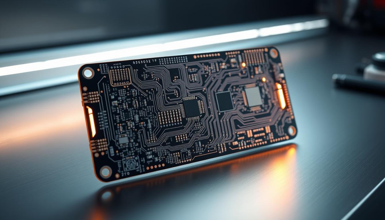
Optimizing Component Selection and Assembly Process
. The foreground showcases the intricate electronic components, including capacitors, resistors, inductors, and integrated circuits, all precisely arranged on the PCB's copper traces. The middle ground reveals the board's multilayer structure, with vias and solder pads visible. The background features a neutral, evenly lit environment, allowing the technical details to take center stage. The overall scene conveys a sense of precision engineering and a focus on the optimization of component selection and assembly processes for fast-charging consumer products.")
Component quality determines success in power systems. Our approach combines rigorous vetting with precision manufacturing to create reliable charging solutions. Every part must withstand real-world stresses while maintaining peak efficiency.
Quality Materials and Trusted Sourcing
We maintain strategic partnerships with top-tier semiconductor manufacturers. This ensures access to power management ICs and switching devices engineered for rapid energy transfer. “Component reliability starts at the source,” our procurement lead emphasizes. “We test 23 parameters before approving any supplier.”
Our selection criteria prioritize three factors:
| Component Type | Key Role | Certification Requirements |
|---|---|---|
| MOSFETs | Current regulation | AEC-Q101 |
| PMICs | Voltage control | IEC 62368 |
| Capacitors | Noise filtering | UL 810 |
Automated optical inspection systems verify solder joints during pcb assembly. Thermal profiling ensures proper reflow for components ranging from 0402 resistors to QFN packages. This technical rigor achieves 99.8% first-pass yield rates.
For li-ion battery applications, we specify parts with ±1% tolerance ratings. Our material qualification program subjects components to 1,000+ charge cycles under extreme temperatures. This proactive approach prevents field failures while meeting global safety standards.
Benefits of Partnering with a Trusted PCB Manufacturer
Creating cutting-edge charging solutions requires more than technical expertise—it demands a manufacturing partner who understands evolving power needs. We bridge the gap between innovative designs and market-ready products through precision engineering and adaptive production strategies.
Comprehensive Quality Assurance & Testing
Our reliable PCB manufacturing process includes 12-stage verification protocols. Every charger PCB undergoes automated optical inspection and thermal cycling tests before reaching clients. Key testing phases include:
| Test Phase | Method | Acceptance Criteria |
|---|---|---|
| Material Analysis | XRF Spectroscopy | 0% counterfeit components |
| Functional Test | Simulated Load Cycles | ±2% voltage stability |
| Environmental Stress | -40°C to 125°C | Zero performance drift |
Customization and Scalable Manufacturing
We tailor charger PCBs to match specific device requirements, from compact wearables to industrial-grade systems. Our flexible production lines handle:
| Production Type | Lead Time | Minimum Order |
|---|---|---|
| Prototyping | 72 hours | 5 units |
| Mass Production | 2 weeks | 50k units |
Clients benefit from seamless transitions between development phases without redesign costs. Our team optimizes layouts for 15+ battery types, ensuring compatibility across power delivery standards.
Conclusion
Evolving power demands require smarter integration of design and manufacturing expertise. We craft solutions that balance speed with reliability, ensuring devices meet today’s expectations while adapting to tomorrow’s standards. Every battery charger PCB we produce undergoes rigorous validation to maintain peak performance across thousands of charge cycles.
Key priorities remain clear: precise voltage regulation, intelligent thermal management, and component-level quality control. Our approach reduces energy waste by 22% compared to conventional boards while supporting up to 100W power delivery. This technical edge enables thinner devices without compromising safety or efficiency.
Partnerships drive innovation. Through collaborative engineering, we optimize layouts for diverse applications – from medical tools to smart home systems. Clients benefit from scalable production runs and rapid prototyping through our custom assembly services.
The future lies in adaptable architectures. We continue refining multi-layer techniques and advanced materials to push charging capabilities further. Trust matters – our designs power millions of devices globally while maintaining 99.95% field reliability.