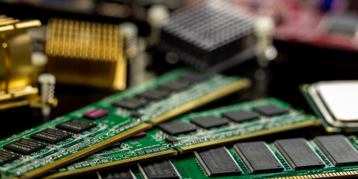
In today’s digital world, every smart device—whether it’s your smartphone, smartwatch, or smart thermostat—runs on a backbone of complex electronics. At the heart of these devices lies something essential but often overlooked: the Printed Circuit Board (PCB). The magic happens when this board is brought to life through a process known as PCB assembly.
Whether you’re a tech startup building your prototype or a manufacturer producing thousands of units, understanding the PCB assembly process, its various types, and its applications is crucial. In this complete guide, we break it all down in simple, easy-to-understand terms.
What is PCB Assembly?
PCB assembly, often abbreviated as PCBA, is the process of populating a blank circuit board (known as a bare PCB) with electronic components to create a functional circuit. This assembled board can then be integrated into an electronic product, allowing it to perform specific tasks.
It’s important to distinguish between PCB (the board itself) and PCBA (the completed, assembled board). The PCB only provides the structure and copper pathways, while the assembly process turns it into a working unit.
The PCB Assembly Process: Step by Step
1. Design and BOM Creation
The process begins with a circuit design created using Electronic Design Automation (EDA) tools. Alongside the design, a Bill of Materials (BOM) is prepared, listing all required components—resistors, capacitors, ICs, connectors, etc.
2. Solder Paste Application
A stencil is used to apply solder paste to the copper pads on the PCB. This paste consists of tiny solder balls suspended in flux, which helps the components adhere to the board during reflow soldering.
3. Pick and Place
Automated machines pick electronic components from reels or trays and place them precisely on the solder-pasted areas. This is mainly done for Surface Mount Devices (SMDs), which are mounted directly on the surface of the PCB.
4. Reflow Soldering
The board passes through a reflow oven, where the solder paste is melted and then cooled, creating permanent joints between the components and the board.
5. Through-Hole Component Insertion (if needed)
For Through-Hole Technology (THT) components, pins are inserted into holes on the board and soldered—either by wave soldering or hand soldering.
6. Inspection and Quality Control
Boards undergo Automated Optical Inspection (AOI), X-ray inspection (for BGAs), and manual visual checks to ensure all components are properly soldered and aligned.
7. Functional Testing
To ensure the board works as intended, it goes through functional tests, including In-Circuit Testing (ICT), Flying Probe Testing, and Functional Testing (FCT) using test jigs and software.
8. Final Assembly and Packaging
Additional steps may include installing connectors, heat sinks, programming microcontrollers, and labeling each unit. After final assembly, boards are cleaned, anti-static packed, and prepared for shipping.
Types of PCB Assembly
- Surface Mount Technology (SMT): Compact, automated, ideal for high-density designs.
- Through-Hole Technology (THT): Strong mechanical bonds, suited for power electronics.
- Mixed Assembly: Combines SMT and THT for optimal performance.
- Single-Sided vs. Double-Sided: Single-sided for simple designs; double-sided or multi-layer for complex, high-density applications.
Applications of PCB Assembly
- Consumer Electronics: Smartphones, TVs, wearables rely on SMT-based assemblies.
- Automotive: ECUs, ADAS, infotainment systems require rugged, reliable PCBA.
- Medical Devices: Pacemakers, diagnostic tools demand high precision and compliance.
- Industrial Equipment: Automation, robotics, sensors use robust mixed assemblies.
- Telecommunications: Routers, base stations leverage multi-layer, high-speed PCBs.
- Aerospace & Defense: Mission-critical electronics undergo stringent testing and certification.
Choosing the Right PCB Assembly Partner
Consider experience, certifications (ISO, IPC, RoHS), testing capabilities, component sourcing, turnaround time, and customer support. A trusted partner ensures smooth production and minimizes costly errors.
Common Challenges in PCB Assembly
Soldering defects, component shortages, thermal stress, and ESD damage can disrupt production. Experienced partners and rigorous testing mitigate these risks.
Final Thoughts
The PCB assembly process is at the heart of modern electronics. From design and sourcing to soldering and testing, each step ensures your product performs reliably. Understanding this process gives you a competitive edge, whether you’re prototyping or scaling up mass production.
