Can a simple coating on the edge of a printed circuit board (PCB) significantly enhance its performance and reliability? The answer lies in edge plating, a specialized technique that applies a metallic coating, typically copper, along the PCB’s edges.
We explore how this process improves electrical connectivity, enhances electromagnetic compatibility (EMC), and supports unique mechanical requirements in modern electronics.
As we delve into the world of PCBs, it becomes clear that every detail in their design can impact their overall functionality. Edge plating creates a continuous conductive path by applying a copper coating along the perimeter edges, connecting top and bottom surfaces.
Key Takeaways
- Edge plating enhances electrical connectivity and improves EMC in PCBs.
- The process involves applying a copper coating along the PCB’s edges.
- It supports unique mechanical requirements in electronic applications.
- Proper design considerations are crucial for successful edge plating.
- Manufacturing implementation and quality control are vital for optimal results.
Understanding PCB Edge Plating
When it comes to PCB design, edge plating is a critical aspect that requires careful consideration to ensure optimal performance. As we delve into the world of PCB manufacturing, it’s essential to understand the role of edge plating in enhancing the electrical and mechanical properties of a circuit board.
What is Edge Plating in PCB Manufacturing?
Edge plating, also known as side plating or castellation, involves electroplating a conductive material—typically copper—along the perimeter edges of a PCB, connecting the top and bottom surfaces. This creates a continuous conductive path that can extend along one or more edges, or even wrap around internal cutouts. The process serves both electrical and mechanical purposes, providing EMI shielding, grounding, and enhancing the durability of the board.
- Edge plating creates electrical connections between the top and bottom surfaces of a PCB.
- It distinguishes itself from standard through-hole plating by focusing on the board’s exterior edges.
- The technique enhances the mechanical durability of the PCB.
The Edge Plating Process Explained
The edge plating process begins during PCB fabrication when the board profile is routed, followed by electroplating during the through-hole plating stage. The thickness of edge plating typically ranges from 25-35 micrometers, though this can be customized based on specific application requirements and electrical performance needs. By understanding the fundamentals of edge plating, engineers can make informed decisions about when and how to implement this technique in their PCB designs.
As we’ve explored, edge plating is a vital process in PCB manufacturing that offers numerous benefits. By applying a conductive material along the edges of a circuit board, manufacturers can create a continuous conductive path that enhances the overall performance of the PCB.
The Importance of Edge Plating in PCB Design
 with a focus on the edge plating feature. The board's layers are clearly visible, showcasing the copper traces, solder mask, and the distinct copper edge plating. The scene is illuminated by a soft, directional light, casting subtle shadows and highlights to emphasize the intricate design. The camera angle is slightly elevated, providing a clear view of the ESPCBA board's edge and the importance of this critical component in PCB manufacturing.")
In modern PCB design, edge plating has emerged as a critical factor for ensuring both electrical and mechanical integrity. Edge plating reinforces the PCB’s perimeter, protecting vulnerable edges from mechanical stress or environmental factors like moisture.
Electrical Benefits of Edge Plating
Edge plating provides critical electrical benefits by creating continuous conductive paths between PCB layers, significantly improving signal integrity in high-frequency applications. It serves as an effective EMI shield, acting as a partial Faraday cage that contains electromagnetic fields within the board’s perimeter. This is essential for RF and wireless communication devices. The technique also creates low-impedance ground connections between layers, minimizing ground loops and providing stable reference points for sensitive analog and digital circuits.
- Improves signal integrity in high-frequency applications
- Acts as an effective EMI shield
- Creates low-impedance ground connections
Mechanical Advantages for PCB Durability
From a mechanical perspective, edge plating reinforces the PCB’s perimeter, protecting vulnerable edges from physical damage, delamination, and environmental factors like moisture. This reinforcement is particularly valuable in rugged applications such as aerospace, automotive, and industrial equipment. Edge plating can significantly extend the operational lifespan of PCBs by preventing edge delamination during thermal cycling and mechanical vibration.
- Protects against physical damage and delamination
- Enhances durability in harsh environments
- Extends PCB lifespan
Key Applications of PCB Edge Plating
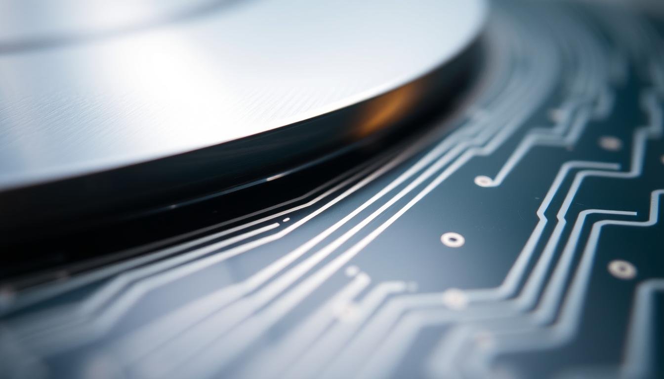
 edge with ESPCBA edge plating for electromagnetic interference (EMI) shielding, viewed from a close and slightly elevated angle. The plating should have a metallic, reflective sheen that seamlessly blends with the PCB surface. The image should showcase the precise edge geometry, intricate plating patterns, and how the shielding material wraps around the PCB sides. Render the scene with soft, directional lighting that accentuates the textures and highlights the technical nature of the subject. Convey a sense of precision engineering and functional elegance.")
The versatility of edge plating is evident in its wide range of applications, from EMI shielding to board-to-board connections. As we explore the various uses of edge plating, it becomes clear that this technology is crucial for enhancing the performance and reliability of modern electronic devices.
EMI Shielding and Signal Integrity
In high-frequency designs, such as RF PCBs operating in the megahertz to gigahertz range, EMI shielding is critical to maintaining signal integrity. Edge plating creates a conductive shield along the board’s perimeter, acting as a partial Faraday cage to contain electromagnetic fields. This is particularly important for applications like wireless communication devices, where signal interference can disrupt performance.
Enhanced Grounding Solutions
For high-speed digital circuits, such as those using low-voltage differential signaling (LVDS) at speeds exceeding 1 Gbps, a stable ground reference is essential. Edge plating connects ground planes across layers, minimizing ground loops and improving signal integrity. This continuous ground connection provides a stable reference point, significantly reducing noise in sensitive analog circuits.
Board-to-Board Connections
Edge plating enables innovative board-to-board connection methods, allowing direct electrical contact between PCBs without requiring additional connectors or components. In modular electronic systems, edge-plated PCBs can slide directly into metal enclosures or card guides, using the plated edge as both a mechanical guide and electrical connector. This approach simplifies the design and enhances the reliability of complex electronic systems.
Design Guidelines for Effective Edge Plating
Designing PCBs with edge plating involves a set of precise guidelines to ensure manufacturability and performance. To achieve optimal results, it’s essential to carefully plan and execute the design.
Defining Plated Areas in Your Layout
To ensure that the edge plating process is successful, we recommend defining plated areas in your PCB layout by using overlapping copper features such as pads, traces, or planes. A minimum overlap of 0.5 mm (20 mils) is suggested to provide sufficient contact for the plating process. For connected layers, maintaining at least 0.3 mm (12 mils) of copper overlap is crucial.
Clearance Requirements and Considerations
Proper clearance is vital to prevent short circuits between the plated edge and other copper features. We advise maintaining a minimum clearance of 0.25 mm (10 mils) between the plated edge and any different-net copper features. Additionally, for power planes, pulling back the plane by at least 0.2 mm (8 mils) from the board edge is recommended to avoid unintended contact.
Solder Mask Removal for Edge Plating
Removing the solder mask along the plated edge is essential for ensuring proper plating and contact with external components. A solder mask pullback of 0.5-1.25 mm (20-50 mils) is typically recommended to expose the copper for plating. This step is crucial for reliable electrical connections.
By following these guidelines, designers can ensure that their PCBs are manufactured with edge plating that enhances both the electrical and mechanical performance of the board. Key considerations include:
- Using overlapping copper features to define plated areas.
- Maintaining proper clearance between plated edges and other copper features.
- Removing solder mask along plated edges for reliable connections.
A Guide to PCB Edge Plating Techniques

The process of edge plating in PCBs is a critical aspect of modern electronics manufacturing, offering numerous benefits. We will explore the various techniques used to achieve effective edge plating, including through-hole plating, selective plating approaches, and surface finish options.
Through-Hole Plating Method
The through-hole plating method leverages the standard PCB fabrication process, where copper is electroplated onto drilled holes and extended to include the board edges. This approach begins with routing the PCB profile where plating is needed, followed by electroplating during the standard through-hole plating stage of manufacturing. By utilizing this method, manufacturers can achieve a robust and reliable edge plating.
Selective Plating Approaches
For applications requiring plating on specific areas of the PCB, selective plating approaches are employed. Techniques like brush plating focus on particular regions by immersing only a portion of the board into the electrolyte solution. Finger-plating is another selective technique, particularly useful for edge connectors, where gold is typically applied over nickel to enhance durability and conductivity.
Surface Finish Options for Edge Plating
Surface finish options play a crucial role in edge plating performance. ENIG (Electroless Nickel Immersion Gold) is often preferred for its excellent corrosion resistance and solderability. For high-durability applications, such as edge connectors, using thicker gold plating (at least 50 microinches) is recommended to withstand thousands of insertion cycles. Understanding these different techniques allows engineers to select the most appropriate edge plating method based on their specific application requirements.
Manufacturing Considerations for Edge-Plated PCBs
To successfully manufacture edge-plated PCBs, designers must be aware of the manufacturing considerations that affect edge plating quality and reliability. The production of edge-plated PCBs involves unique challenges that necessitate careful planning and communication with fabricators.
Communicating Edge Plating Requirements to Fabricators
Clear communication of edge plating requirements to PCB fabricators is crucial to avoid misunderstandings and manufacturing delays. We emphasize the importance of detailed fabrication drawings and notes to ensure that our requirements are properly understood. For instance, including a note such as ‘PLATING TO BE ALONG BOARD EDGE. FINISHED THICKNESS OF EDGE PLATING TO BE X MILS +/- Y MILS’ in the fabrication documentation can significantly reduce errors.
Common Manufacturing Challenges and Solutions
Several manufacturing challenges can impact the quality of edge-plated PCBs. These include burr formation from routing operations and peeling of plated copper due to poor adhesion. To address these issues, we can specify advanced deburring techniques like chemical etching or polishing and request roughened edge surfaces and high-bond-strength metallization processes.
| Challenge | Solution |
|---|---|
| Burr formation from routing | Advanced deburring techniques (chemical etching or polishing) |
| Peeling of plated copper | Roughened edge surfaces and high-bond-strength metallization |
| Interference from vias or plated holes near edge | Maintain minimum clearance of 0.25mm (10 mils) |
Advanced Applications and Industry Uses
Edge plating has become a crucial aspect in various advanced PCB applications, enhancing performance and reliability across different industries. We observe that edge plating is particularly beneficial in high-frequency and high-power applications.
RF and High-Frequency PCB Applications
In RF and high-frequency PCBs, edge plating provides superior EMI shielding, which is critical for maintaining signal integrity. For instance, in 5G antenna modules, edge plating creates a continuous ground path that significantly reduces electromagnetic interference, ensuring signals remain clean even at frequencies above 3 GHz. This technique helps maintain controlled impedance by providing consistent ground references and minimizing radiation losses.
Thermal Management Solutions Using Edge Plating
Edge plating also offers effective thermal management solutions for high-power applications. By connecting edge plating to ground planes via thermal vias, it creates an efficient heat dissipation path. This is particularly valuable in applications such as LED lighting or power supplies, where significant heat is generated. For example, in an automotive power module, edge plating can reduce the temperature of a 100 W circuit by up to 10°C, extending component lifespan.
- Edge plating enhances EMI shielding in RF and high-frequency applications, ensuring signal integrity.
- It provides a continuous ground path in 5G antenna modules, reducing electromagnetic interference.
- Edge plating helps maintain controlled impedance and minimizes radiation losses in RF applications.
- In high-power applications, edge plating connected to ground planes via thermal vias improves heat dissipation.
- This technique can reduce operating temperatures in automotive power modules by up to 10°C.
Conclusion
In conclusion, edge plating is a powerful tool that can significantly enhance PCB performance across multiple dimensions, including EMI shielding, signal integrity, thermal management, and mechanical durability.
By understanding its applications and adhering to design guidelines, engineers can unlock the full potential of edge plating while avoiding common pitfalls. Effective collaboration with fabrication experts is crucial for achieving high-quality results.
As electronics continue to evolve toward higher frequencies and more compact form factors, edge plating will remain a critical technique in the PCB designer’s toolkit, enabling the creation of robust and reliable printed circuit boards.