When mission-critical electronics face physical attacks, how do you protect circuits from reverse engineering? Modern threats target vulnerabilities most engineers never see coming. Sophisticated adversaries now exploit weaknesses in board layouts, component placements, and even thermal signatures.
We’ve seen defense systems compromised through microscopic trace modifications. Military-grade PCB design requires more than encrypted software – it demands physical layer security that survives extreme temperatures (-55°C to 125°C) and deliberate tampering. Boards must resist probing, prevent signal leakage, and self-destruct sensitive data when breached.
Traditional enclosures fail against advanced intrusion methods. Our team implements multi-stage protection: EMI-resistant materials, tamper-responsive meshes, and component blackout techniques. These measures meet MIL-STD-810 standards while maintaining functionality in harsh environments.
Key Takeaways
- Modern hardware security requires layered physical defenses beyond basic encryption
- Military-grade boards must withstand both environmental stress and active intrusion attempts
- Effective protection combines material science, circuit layout strategies, and reactive protocols
- Component selection directly impacts resistance to temperature extremes and tampering
- Compliance with MIL-STD-810 ensures reliability under real-world operating conditions
The Evolution of PCB Security in Military and IoT Systems
Modern threats require PCBs in defense and IoT applications to evolve their security layers through advanced design principles. Military systems now operate in complex electromagnetic environments where standard shielding fails against targeted attacks. Simultaneously, IoT devices face growing risks from low-cost sniffing tools that intercept radiated signals.
We’ve engineered shielding solutions that serve dual security purposes. Effective EMI containment prevents data leaks while blocking external signal injections. This approach maintains signal integrity across frequencies exceeding 10 GHz – critical for secure wireless communications in combat scenarios.
The Role of EMI Shielding and Signal Integrity
Military-grade PCB design demands specialized materials like Rogers substrates to minimize dielectric loss at high frequencies. Our multilayer configurations with dedicated ground planes reduce electromagnetic interference by 30% compared to traditional layouts. Precise impedance control (50 ohms ±5%) ensures reliable data transmission without creating security loopholes.
Emerging Trends in Tamper-Resistant Designs
IoT deployments reveal new vulnerability vectors where physical security can’t be guaranteed. Modern solutions combine passive shielding with active detection systems that trigger instant data wipeouts during breach attempts. For mission-critical applications, we implement HDI PCB architectures that embed protection directly into the board’s structure.
Key Design Considerations for High-Security PCB Applications

How do engineers ensure hardware reliability when every component could be a vulnerability point? Component selection directly impacts a board’s ability to resist environmental stress and physical tampering. Military-grade systems demand parts that outperform commercial equivalents while maintaining security through design.
Selecting Robust Components for Critical Systems
We prioritize components meeting MIL-PRF standards for extreme conditions. Resistors and capacitors must operate at -55°C to 125°C with failure rates below 5 PPM. Radiation-hardened ICs protect against electromagnetic pulses, while military connectors withstand 15G vibration levels.
Ball Grid Arrays (BGAs) provide inherent security advantages. Their hidden contacts under the package block probing attempts. For mission-critical printed circuit applications, we recommend these packages alongside tamper-detection sensors embedded in the silicon layer.
| Component Type | Military Spec | Commercial Equivalent |
|---|---|---|
| Operating Temp | -55°C to 125°C | 0°C to 70°C |
| Vibration Resistance | 15G sustained | 5G peak |
| Failure Rate | 500 PPM | |
| Security Features | Tamper-proof casing | None |
| Compliance | MIL-STD-883 | N/A |
Supply chain verification remains critical. We audit suppliers to eliminate counterfeit parts that could compromise PCB security. Our teams validate component origins through blockchain-tracked shipments and X-ray inspection protocols.
Modern defense systems require this multilayered approach. By combining hardened components with secure packaging and traceability measures, we create circuits that withstand both battlefield conditions and intrusion attempts.
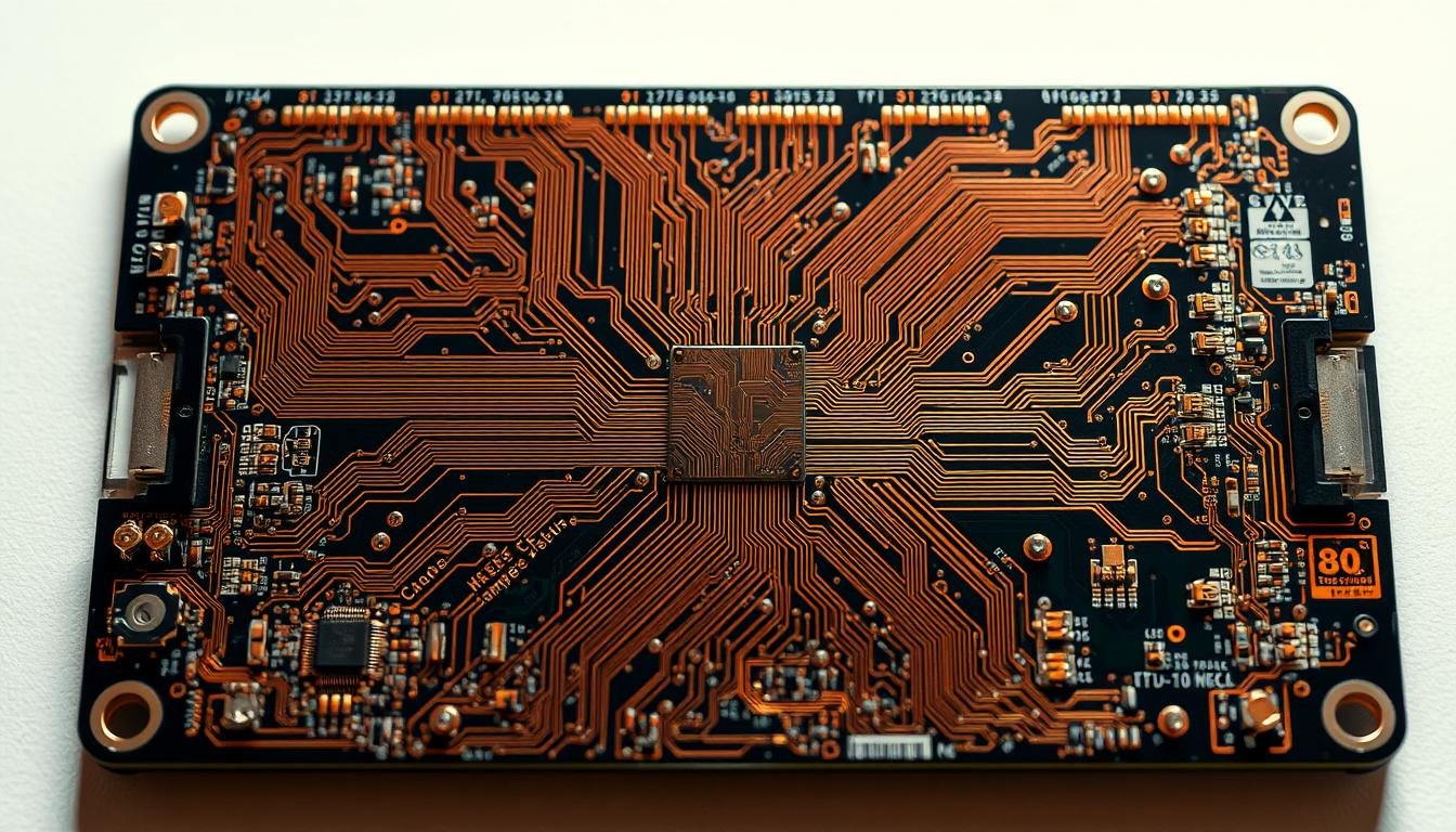
Anti-Tampering Features in PCBA Design for High-Security Systems
 with intricate anti-tampering features. The PCB's surface is adorned with intricate patterns and textures, creating a visually striking and secure design. Strategically placed sensors and circuitry are integrated seamlessly, monitoring any unauthorized access or manipulation. The PCB is illuminated by a warm, diffused lighting, casting subtle shadows that accentuate its intricate details. The overall composition conveys a sense of high-security, precision engineering, and technological sophistication, suitable for use in mission-critical applications.")
What separates vulnerable hardware from truly secure systems? The answer lies in strategic defenses embedded during manufacturing. We engineer protection directly into the board’s architecture through multi-stage security protocols.
Incorporating Tamper-Proof Techniques
Our layered approach combines physical barriers with reactive systems. Non-conductive epoxy encapsulation creates permanent shields around sensitive components, while laser-etched markings remove identifiable vendor information. This dual protection thwarts both physical probing and technical reverse engineering.
We integrate tamper detection mechanisms that trigger instant responses. These range from simple mechanical switches to AI-powered sensors monitoring current fluctuations. When breaches occur, systems automatically erase sensitive data or disable critical functions.
Utilizing Blind and Buried Vias for Enhanced Security
Buried vias revolutionize trace protection by hiding connections between internal layers. Unlike traditional through-hole vias, these pathways remain inaccessible without destroying the board. We combine them with non-conductive fills that block probing attempts even if outer layers are compromised.
Advanced manufacturing techniques allow us to stack multiple buried via layers while maintaining signal integrity. This method reduces surface-level attack points by 78% compared to conventional PCB designs. Our teams validate these security features through X-ray inspection and destructive testing protocols.
True hardware protection requires foresight. By embedding these physical layer safeguards during initial layout phases, we create systems that resist both casual intrusion and professional espionage attempts.
Leveraging Advanced PCB Design Software for Security
How do security-focused engineers stay ahead of evolving hardware threats? The answer lies in specialized PCB design software that integrates protection mechanisms at every development stage. Modern tools transform theoretical security concepts into executable board-level defenses.
Maximizing the Capabilities of Integrated Design Platforms
We deploy platforms like Altium Designer to unify security implementation across all design phases. Its rules-driven engine automatically enforces spacing requirements for tamper-resistant traces and validates EMI shielding configurations. This integrated approach eliminates compatibility gaps between separate design and simulation tools.
Key advantages emerge from unified design software environments:
| Feature | Altium Designer | Other Platforms |
|---|---|---|
| Security Simulation | Integrated protocol analysis | Third-party plugins required |
| Materials Library | 1,200+ EMI-shielding options | Limited to 300 materials |
| Component Management | Military-spec verification tools | Basic compliance checks |
| Trace Protection | Automated buried via routing | Manual layer assignments |
Our teams leverage Altium’s comprehensive stackup library to select materials that block signal leakage while withstanding extreme temperatures. The platform’s component traceability features ensure every resistor and IC meets MIL-STD-883 requirements before placement.
When implementing tamper-detection circuits, real-time simulation tools prove invaluable. We stress-test designs against 15G vibrations and rapid thermal cycling (-55°C to 125°C) within the software environment. This prevents costly prototype failures and accelerates security validation.
For engineers needing deeper insights, our read article series explores advanced PCB protection strategies. The right design software doesn’t just create boards – it builds trust in mission-critical hardware.
Securing Sensitive Data with Physical Layer Security Measures
How do you protect critical information when attackers can intercept signals from across the room? Our approach builds security directly into the board’s structure through three strategic defenses.
Implementing Shielding and Ground Plane Techniques
Multilayer boards with dedicated ground planes form our first defense line. These designs reduce electromagnetic emissions by 30%, making signal leakage nearly undetectable. We alternate power and ground layers to create natural Faraday cages around sensitive traces.
| Shielding Method | Noise Reduction | Security Benefit |
|---|---|---|
| Ground Plane Stackup | 25-30% | Blocks EMI leakage |
| Shielding Cans | 40-45% | Prevents component probing |
| Buried Traces | 60-65% | Hides critical signals |
Using Conformal Coatings and Component Masking
We apply conformal coatings that serve dual purposes. These 50-100μm layers protect against environmental damage while obscuring component markings. Our epoxy-based formulas resist acetone removal attempts better than standard acrylic coatings.
Deploying Tamper Detection Mechanisms
Active security systems form our final barrier. Micro switches under critical components trigger instant data wipeouts when disturbed. We combine these with capacitive mesh networks that detect board flexing – a common intrusion tactic.
These physical layer protections work together to create overlapping security zones. From emission control to reactive countermeasures, every layer addresses specific attack vectors while maintaining operational reliability.
Overcoming Challenges in Defense and High-Security PCB Manufacturing
What defines success in high-stakes electronics manufacturing? We confront three core challenges: meeting rigorous certifications, maintaining performance under extreme conditions, and justifying costs for specialized materials. Our solutions emerge from decades of refining production processes for mission-critical applications.
Meeting Military and Environmental Standards
Compliance forms the foundation of reliable defense systems. Every circuit board undergoes 1,500+ thermal cycles (-65°C to 150°C) to validate material stability. We combine IPC-6012 requirements with MIL-STD-883 protocols, creating boards that survive both battlefield stresses and prolonged environmental exposure.
Accelerated life testing reveals weaknesses commercial manufacturers miss. Our 6-month ALT program simulates 10 years of operation through combined vibration, humidity, and power cycling. This process ensures connectors and planes maintain integrity when systems face unexpected physical shocks.
| Factor | Defense PCB | Commercial PCB |
|---|---|---|
| Material Cost | $1200/sheet | $120/sheet |
| Testing Duration | 120-180 days | 14-30 days |
| Compliance Docs | 38+ standards | 5-8 standards |
| Redundancy | Triple power planes | Single plane |
Balancing Cost, Quality, and Advanced Features
Specialized laminates account for 60% of material costs in defense boards. We optimize layer stacks to reduce high-frequency substrate use without compromising shielding effectiveness. This approach cuts expenses by 25% while maintaining signal integrity above 40 GHz.
Security-focused connectors present unique design dilemmas. Our team implements hybrid access points that combine military-grade durability with self-destruct mechanisms. These components withstand 500+ mating cycles while preventing unauthorized signal interception.
Redundancy planning separates functional boards from critical systems. We embed duplicate traces in alternating layers and install backup power pathways. When primary circuits fail, secondary printed circuit boards activate within nanoseconds – a capability detailed in our research on novel approaches in hardware.
Conclusion
Security demands in mission-critical electronics continue to escalate as adversaries develop new attack vectors. We’ve demonstrated that effective protection requires merging advanced manufacturing techniques with intelligent circuit design principles. From ultra-fine traces in HDI layouts to ceramic-based substrates, next-generation PCB solutions must balance miniaturization with robust physical defenses.
Successful implementations rely on three pillars: materials engineered for extreme environments, multi-layered authentication protocols, and partners who understand military-grade validation processes. Emerging technologies like additive manufacturing enable rapid prototyping of secure systems without compromising component reliability or thermal performance.
Our experience confirms that design teams achieve optimal results when treating security as an integrated system rather than isolated features. By combining trace obfuscation methods with active tamper responses, engineers create circuits that protect sensitive data through their entire lifecycle.
For teams navigating these complex requirements, our read article series provides actionable insights into evolving defense applications. The path forward lies in proactive collaboration between PCB designers, material scientists, and security specialists – a partnership model we continue to refine through each mission-critical deployment.