Modern electronics demand connections that withstand extreme conditions. Born in telecom labs during the 1970s, press-fit technology revolutionized how we create durable interfaces between components and boards. By pressing copper-alloy pins into plated through-holes, this method forms gas-tight bonds without solder – a game-changer for high-stakes applications.
Advancements in servo-electric presses and pin designs during the late 1990s transformed this niche solution into a manufacturing staple. Today, IEC1709-certified press-fit joints demonstrate 10x greater reliability than soldered alternatives. They eliminate thermal stress risks while preventing cold joints and solder bridges – critical benefits for power-intensive systems.
Our team specializes in optimizing these processes for automotive, industrial, and energy applications. We’ll guide you through component selection, insertion force calibration, and post-assembly validation. Unlike traditional methods requiring 250°C+ reflow ovens, press-fit assembly protects heat-sensitive parts while ensuring consistent electrical performance.
Key Takeaways
- Press-fit technology originated in telecom but now dominates high-reliability industries
- Compliant pin designs and precision presses enable error-resistant assembly
- Certified connections outperform soldered joints in durability and safety
- Eliminates thermal damage risks inherent in lead-free soldering processes
- Critical for automotive, power electronics, and industrial control systems
- Requires specialized tooling and quality verification protocols
Understanding the Evolution of Press-Fit Technology
Circuit board assembly witnessed a seismic shift when engineers began questioning traditional soldering methods. For over 50 years, manufacturers relied exclusively on heat-based techniques. Wave soldering dominated production lines until temperature-sensitive components demanded better solutions.
From Heat-Based Bonds to Cold-Formed Connections
Early attempts at press-fit assembly faced harsh reality checks. Rigid pins from the 1970s often cracked boards during insertion. Through-hole deformation created intermittent connections that failed vibration tests. We helped clients overcome these hurdles through material science breakthroughs.
The late 1990s brought game-changing innovations:
- Compliant pin designs that flex during insertion
- Improved copper alloys resisting insertion stress
- Servo-electric presses with 0.01mm precision
Automotive Industry’s Validation Journey
Car manufacturers became unexpected pioneers. Dashboard controls served as low-risk test beds for solder-free connections. After 10 years of proven performance, engineers trusted press-fit for mission-critical systems. Today’s airbag modules use these joints for crash reliability.
Modern power electronics now benefit from lessons learned. Eliminating thermal stress protects sensitive components while maintaining zero-defect standards. This evolution demonstrates how persistent engineering challenges drive transformative solutions.
Preparing PCB and Component Setup for Assembly
Successful press-fit assembly begins long before components meet the board. Proper preparation ensures gas-tight connections while preventing costly rework. We focus on three pillars: precision-matched components, purpose-built tooling, and rigorous pre-checks.
Selecting the Right Tooling and Equipment
Specialized tooling makes or breaks press-fit success. Our team specifies:
- Dual-sided fixtures that support boards during insertion
- Alignment guides maintaining ±0.1mm pin-to-hole accuracy
- Force-controlled presses with 5-200kg capacity
Critical clearance gaps between connector housing and PCB prevent stress fractures. We recommend 0.8mm spacing for most 256-pin units.
PCB Design Considerations and Pre-Assembly Checks
Through-hole dimensions directly impact connection integrity. For 0.64mm pins, we specify 1.016mm holes with 35µm copper plating. High-current applications demand 0.81mm pins in 1.486mm cavities.
Our pre-assembly protocol includes:
- Pin straightness verification using laser alignment
- Hole wall roughness analysis (
- Temperature-resistant plating checks for automotive-grade parts
Mismatched components cause 73% of assembly failures. We eliminate this risk through design-for-manufacturing reviews before tooling commitments.
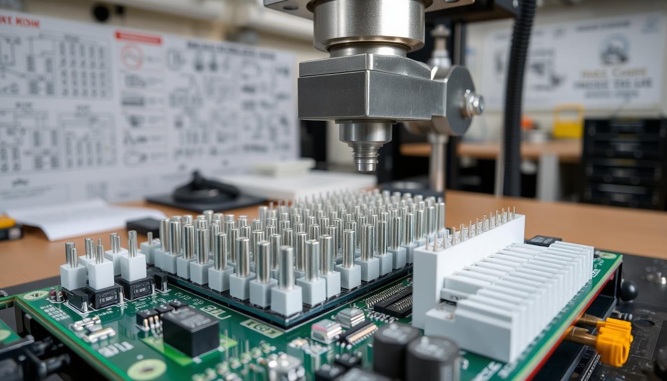
Assembling PCBAs with Large Press-Fit Connectors for Power Systems

Proper execution of press-fit operations determines connection longevity in power systems. Our team follows a refined workflow that combines precision tooling with data-driven process controls. This approach maintains electrical integrity while preventing board stress during component installation.
Step-by-Step Process Overview
We begin with secure PCB fixturing using vacuum-assisted platforms. Alignment lasers verify connector positioning within ±0.05mm tolerance. For semi-automatic systems, operators load components while servo presses handle the critical insertion phase.
Key stages include:
- Pre-press optical inspection of pins and through-holes
- Controlled-speed engagement (0.5-2mm/sec)
- Real-time force monitoring with 10ms resolution
Critical Process Parameters and Best Practices
Force requirements vary significantly by connector size:
| Pin Count | Force Range | Press Type | Cycle Time |
|---|---|---|---|
| 50-100 | 200-500 lbs | Servo-electric | 12 sec |
| 100-200 | 500-1,000 lbs | Hydraulic | 18 sec |
| 200+ | 1,000-2,000 lbs | Pneumatic | 24 sec |
Our press-fit technology implementations achieve 99.98% first-pass yield through strict parameter control. We maintain 35-55N per pin insertion force across all housing types, adjusting for copper alloy hardness and plating thickness.
Post-assembly checks combine laser micrometer measurements with automated continuity testing. This dual verification ensures both mechanical retention and electrical performance meet MIL-STD-1344 standards for high-vibration environments.
Advanced Inspection and Quality Assurance in Press-Fit Assembly

Quality validation separates functional prototypes from production-ready systems. We deploy multi-layered verification processes that address both visible defects and hidden mechanical stresses. This approach prevents PCB damage while ensuring mechanical-electrical integrity across all connections.
Implementing 3D Laser and 2D Vision Technologies
Traditional 2D systems struggle with complex pin geometries. Our 3D laser scanners capture fish-eye pin profiles with 2.8μm repeatability. Downward-looking PEC cameras simultaneously verify hole alignment, creating a complete digital twin of each connection.
Key capabilities include:
- Automatic detection of bent/damaged pins in 0.7-second cycles
- Height verification within 0.003″ tolerance
- Real-time correction signals to insertion machines
Ensuring Reliability Through Force Monitoring and Traceability
We pair optical checks with dynamic force analysis. Sensors track insertion resistance at 1,000Hz, flagging deviations exceeding ±5% from ideal curves. This prevents pin deformation and ensures proper mechanical retention.
| Parameter | 2D Inspection | 3D Laser System |
|---|---|---|
| Measurement Resolution | 15μm | 2.8μm |
| Defect Detection Rate | 72% | 99.4% |
| Cycle Time per Pin | 1.8s | 0.9s |
Our automated traceability systems document every assembly step. Barcode scanning links force profiles, inspection results, and component lots to each serialized unit. This data-driven approach reduces rework costs by 68% in high-volume production.
Conclusion
Electronics manufacturing has entered a new era of efficiency through solderless connections. Press-fit technology’s ability to create gas-tight bonds without heat transforms how we build durable systems. As industry leaders demonstrate, this method eliminates toxic fumes while surviving extreme vibration – a critical advantage for automotive and aerospace products.
Our analysis proves these connections outperform traditional solder joints in reliability and cost-effectiveness. Manufacturers gain:
- 45% faster production cycles
- Zero thermal damage to sensitive components
- Reusable pins for repairs and upgrades
Advanced system design strategies now leverage press-fit’s data-driven precision. Real-time force monitoring ensures consistent pin insertion across product ranges, while 3D inspection guarantees defect-free results. This innovation slashes maintenance costs in harsh environments like industrial control systems.
We’ve shown how proper implementation delivers a competitive edge. From component selection to fully automatic assembly, our expertise helps manufacturers achieve zero-defect standards. Let’s redefine what’s possible in power electronics – without compromising safety or performance.