As bare PCBs are custom products, pricing depends on the material, layers, and surface finishes. Contact us with your PCB files for a quote.
16+ Years Experience in PCB Manufacturing
- 1-40 Layers of Rigid, Flex, and Rigid-Flex
- FR4, High-Speed, High-Frequency, Metal Core, Ceramic, PTFE
- Blind & Buried Vias, Micro Vias, Any-Layer HDI
- Conductive & Non-Conductive Via Plugging
- Back Drill, Backplane, Embedded Devices, IC Substrate
- Quick Turn Bare PCB in 24 Hours
Get a free quote now!
What is a Bare PCB?

Get a free quote now!
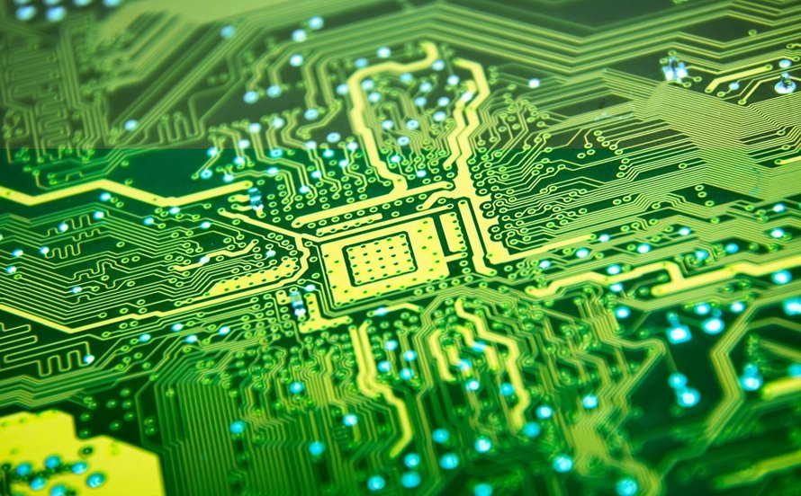
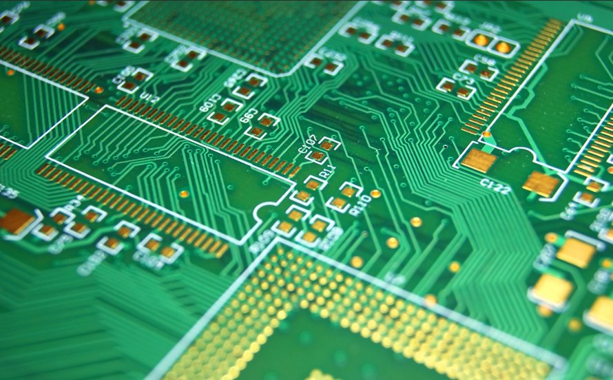
A bare PCB, also known as a PCB bare board, is a fully fabricated printed circuit board (PCB) that includes copper traces and vias to establish electronic connections. Essentially, a bare PCB lacks mounted components and is sometimes referred to as a raw PCB. Despite its appearance, the bare PCB is a crucial part of the manufacturing process since many tests and procedures are carried out on it before component assembly. However, a bare PCB cannot perform its intended functions until components are added and tested for the required functionality.
Components of a Bare PCB:
- Substrate or Base Material: Provides insulation between copper layers and maintains the PCB’s structural integrity.
- Copper Layer: Houses the traces and nets necessary for routing.
- Solder Mask: Protects the copper traces during assembly.
- Silkscreen: Displays text and symbol markings, usually in white.
- Surface Finishes: A protective layer on exposed copper and pads, including finishes like HAL, ENIG, OSP, immersion silver, immersion tin, and ENEPIG.
Difference Between Bare PCB and Zero PCB
Although similar in appearance, a bare PCB and zero PCB are distinct. A bare PCB is a custom-designed circuit board without components, while a zero PCB is a general-purpose board for small applications, with holes arranged in a grid pattern but lacking solder mask and silkscreen. The zero PCB functions similarly to a breadboard, used for testing small circuits.
Bare PCB Manufacturing Process
The manufacturing or fabrication of a bare PCB follows a detailed and systematic process:
Generating Design and Output Files:
After creating a schematic on EDA tools and generating a PCB layout, a Gerber file is produced along with a fabrication note (Fab note). Once all design checks are completed, the file is sent for production.
Generating Films:
The Gerber file undergoes DFM checks, and a plotter produces detailed films of the PCB design on plastic sheets for each solder mask and layer.
Printing the Layers:
A copper-clad laminate is used, over which the design is printed using photo-negative prints. The layout is then hardened with photoresist under UV light, and the unwanted copper is removed.

Removing Unwanted Copper:
Excess copper is washed away, leaving the desired traces.
Layer Bonding:
The layers are pressed together with core and prepreg as per the stack-up in the fabrication note.
Copper Plating:
The PCB undergoes copper and tin plating to protect the traces before the final etching.
Applying Solder Mask:
A solder mask is applied and cured under UV light.
Printing Silkscreen:
Silkscreen is printed on the top and bottom surfaces.
Separating Bare PCB from the Panel:
The PCB is separated from the panel using a V groove or router.
Visual Inspection:
Each layer is thoroughly inspected against the Gerber file to ensure accuracy.
Drilling:
The board is drilled as per the coordinates defined in the design, preparing it for plating.
Final Etching:
The board is etched one last time to finalize the traces.
Surface Finishing:
Surface finishes are added for solderability and durability.
Testing:
Electrical testing is conducted to ensure the PCB meets manufacturer and designer standards.
Electrical Tests for Bare PCBs
Before being commissioned, bare PCBs undergo several electrical tests, adhering to IPC 9252 standards:
- Resistance Test: Measures resistance across nets.
- Isolation Test: Verifies insulation between nets to prevent short circuits.
- Capacitance Test: Measures capacitance between points on the PCB.
- Continuity Testing: Confirms that there are no breaks in the connections.
- Flying Probe Test: A quick, reliable test for continuity, short circuit detection, and impedance verification.
- 4-wire Kelvin Test: Used for precise measurement of low resistances, especially in advanced PCBs.
ESPCBA: Your Trusted Partner for Bare PCB Fabrication
At ESPCBA, we ensure a seamless development process for your bare PCBs:
Expert Design Review:
Our experienced team reviews your design for manufacturability and addresses any potential concerns.
High-Quality Production:
We manufacture PCBs with precision, leveraging a trusted network of suppliers.
Advanced Fabrication Processes:
We offer advanced techniques like impedance control, blind and buried vias, and more.
Full Assembly Integration:
Easily transition from bare PCBs to fully assembled boards.
Connect with us
Get an Instant Online Quote Today
Looking for reliable SMD assembly services? At ESPCBA, we’re your trusted partner for PCB fabrication, component sourcing, and electronic manufacturing. With over 16 years of experience, we’ve provided high-quality PCBs at competitive prices to over 1,000 customers worldwide. Our company is ISO9001:2015 certified and UL listed, and every product we deliver is 100% E-tested and inspected using AOI and X-ray to meet the highest standards. Get an instant quote from our sales team today, and let us handle the rest for you.
Frequently Asked Questions
A bare PCB is an unpopulated printed circuit board, meaning it lacks any components.
Visual inspection is the first step, checking for any physical damage. For finer details, microscopes may be used, and electrical testing follows to verify connections and performance.
Yes, by making electrical connections between the bare PCB and external devices, it can be controlled manually or through code to function as an input device.
No, mixing lead-free and leaded materials can cause corrosion and compatibility issues.
ESPCBA offers competitively priced, high-quality bare PCBs with excellent customer service and fast turnaround times.
A bare PCB must withstand electrical discharges without compromising performance. ESD testing ensures the PCB can handle these discharges safely.
- Lower cost
- Greater layout flexibility
- Enhanced electrical performance
- Higher component density
- Easier prototyping
Consider factors such as size, layers, copper thickness, material, and trace widths when choosing the right PCB for your project.
The process includes designing, etching, cleaning, and adding protective coatings to create a functional bare PCB.
Stored properly, bare PCBs can last up to 3 years, depending on the materials used.
Yes, we offer a variety of bare LED PCBs, including FR4, aluminum, metal core, and ceramic options.
We conduct several tests, including dedicated fixture testing, flying probe testing, and universal bare board testing.
A bare PCB is unpopulated, while a populated PCB has all components assembled and ready for use.