High-Quality Capacitive PCBs at Competitive Prices
- PCB Types: Rigid PCB, Flexible PCB, Rigid-Flex, Semi-Flex
- Material: FR4, High-Speed, High-Frequency, Microwave
- Impedance Control with 5% Tolerance
- Blind & Buried Vias, Micro Vias, HDI
- ISO9001:2015 Certified & UL Listed
- Standards: IPC-A-600 Class 2, Class 3
Capacitive PCBs play a crucial role in modern electronics, thanks to their ability to detect changes in electrical capacitance. These PCBs are integral to touch-sensitive devices, powering innovations from smartphone screens to interactive kiosks.
Get a free quote now!
What is a Capacitive PCB?
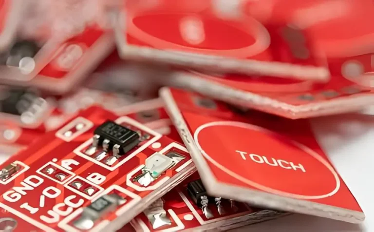
Also known as a capacitive sensor PCB, a capacitive PCB is specially designed to detect and measure changes in electrical capacitance caused by the proximity or touch of a finger or conductive object. These PCBs are foundational in creating touch interfaces for various electronic devices.
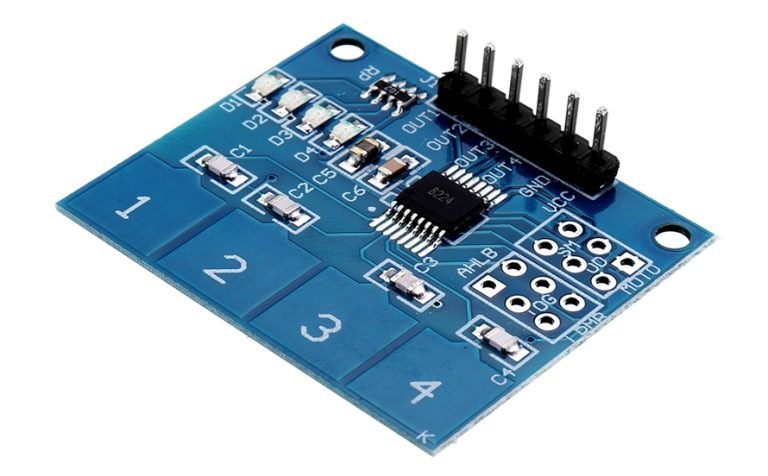
The core components of a capacitive PCB include conducting traces, dielectric materials, and a controller chip that translates capacitance changes into actionable data. The insulating material used in these PCBs is chosen for its capacity to allow capacitive signals to pass through. FR4 is a common substrate material, typically combined with conductive copper layers.
Get a free quote now!
How Do Capacitive PCBs Work?
Capacitive PCBs operate based on the capacitance effect, which is the system’s ability to store electric charges. This principle involves a conductive layer and dielectric materials. Here’s how it works:
Capacitive PCBs are made of multiple layers, with conductive materials serving as capacitive plates and dielectric materials supporting electrostatic fields.
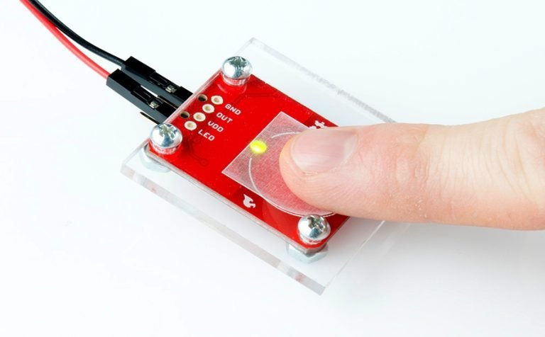
When a user touches the sensor PCB surface, the capacitance between the plates changes.
The PCB sensors detect capacitance changes and convert the touch into an electrical signal, processed by a controller chip to determine the location and type of touch.

The interaction between conductive layers and dielectric materials influences the sensitivity and accuracy of the PCB. The type and thickness of the dielectric material impact capacitance, affecting the touch interface’s responsiveness.
These PCBs support various touch-sensitive applications, from simple buttons to complex touchscreen interfaces found in smartphones and tablets. Carefully chosen materials ensure optimal performance for each application. Combining advanced signal processing with well-balanced materials, capacitive PCBs enable reliable user interactions across a wide range of devices.
Benefits of Capacitive PCBs
Capacitive PCBs significantly improve interface sensitivity, allowing for sophisticated and responsive touch interactions. They are essential for enhancing the user experience in devices requiring frequent interaction.
Capacitive PCBs react instantly to touch, making them ideal for applications like gaming consoles and interactive displays.
These PCBs are well-suited for IoT devices and flexible electronics, enabling innovations in smart wearables and other new technologies. Capacitive PCBs continue to drive technological progress, fostering new developments across various industries.

Applications of Capacitive PCBs
Capacitive PCBs are fundamental in smartphones and tablets, enabling smooth touchscreen technology for browsing, gaming, and other applications.
Capacitive PCBs power interactive interfaces in wearables like smartwatches and fitness trackers, enabling users to navigate menus and access information with a simple touch.
Capacitive PCB technology enhances automation systems by improving efficiency, safety, and precise control.
Design and Manufacturing Process of Capacitive PCBs
Design Considerations
Key factors in capacitive PCB design include sensitivity, device size, shape, and power consumption. The design must balance responsiveness with power efficiency, especially for battery-operated devices.
Layout and Spacing Considerations
- Electrode Configuration: Proper electrode arrangement is essential for accurate touch detection. Incorrect placement can lead to signal interference.
- Trace Width and Spacing: Reducing trace width and increasing spacing minimizes capacitive coupling, improving performance.

Manufacturing Overview
- Material Selection: The process begins with selecting the substrate and conductive materials to meet design specifications for capacitance and durability.
- Layer Stacking: Layer stacking requires precise placement of conductive and dielectric layers to ensure optimal functionality.
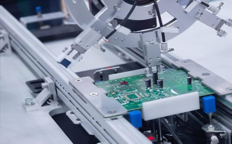
- Etching: Etching removes conductive material to form traces and electrodes. This process must be performed with precision to preserve the design.
- Testing: Each board undergoes rigorous testing to ensure functional performance, particularly for capacitive properties and accuracy.
Production Challenges
- Etching Precision: Capacitive PCBs require extremely accurate etching, increasing production costs due to the high precision needed.
- Material Consistency: Strict quality control is necessary to maintain consistency between dielectric and conductive materials, as variations can affect capacitance.
- Component Integration: Careful assembly is required to ensure that other components do not interfere with the capacitive properties of the PCB.
Challenges in Capacitive PCB Implementation
Capacitive PCBs require highly precise manufacturing due to their complex design patterns. This complexity can affect functionality and yield, necessitating continuous engineering innovation to support miniaturization without sacrificing performance.
Capacitive PCBs are sensitive to environmental factors such as temperature, humidity, and electromagnetic interference. Protective coatings and material selection are essential to mitigate these effects.

Special materials and advanced manufacturing processes increase the production cost of capacitive PCBs compared to standard PCBs. The precision required in etching and testing further contributes to these higher costs.
Addressing these challenges requires a deep understanding of both technical and economic factors, ensuring capacitive PCB technology continues advancing while maintaining broad applicability.
ESPCBA Can Bring Your Ideal Capacitive PCBs to Life
Unlike traditional PCBs, capacitive PCBs interact directly with users, offering highly responsive touch interfaces. Their growing importance is evident in their widespread adoption across many technologies. Given their technical complexity, you need a reliable team to develop capacitive PCBs. ESPCBA is your ideal partner, offering numerous advantages:
Advanced manufacturing technology
Industrial-grade quality assurance
Flexible communication and production processes
Timely delivery
Comprehensive one-stop service
Competitive pricing
Connect with us
Get an Instant Online Quote Today
Looking for reliable SMD assembly services? At ESPCBA, we’re your trusted partner for PCB fabrication, component sourcing, and electronic manufacturing. With over 16 years of experience, we’ve provided high-quality PCBs at competitive prices to over 1,000 customers worldwide. Our company is ISO9001:2015 certified and UL listed, and every product we deliver is 100% E-tested and inspected using AOI and X-ray to meet the highest standards. Get an instant quote from our sales team today, and let us handle the rest for you.
Frequently Asked Questions
A capacitive PCB uses capacitive sensing to detect touch or proximity inputs.
Capacitive PCBs detect changes in electrical capacitance when touched by a conductive object like a human finger.
- No physical contact needed
- High accuracy and sensitivity
- Durability for long-term use
- Quick response times
- Energy-efficient and cost-effective
Consider the manufacturer’s experience, skilled team, competitive pricing, and responsive customer service.
The process includes diagram generation, PCB layout design, copper trace routing, and more.
Key steps include board cutting, drilling, copper etching, solder mask printing, and quality testing.
These include complex designs, advanced fabrication processes, and higher costs.
Check connections, soldering, and EMI protection, and replace damaged components if necessary.