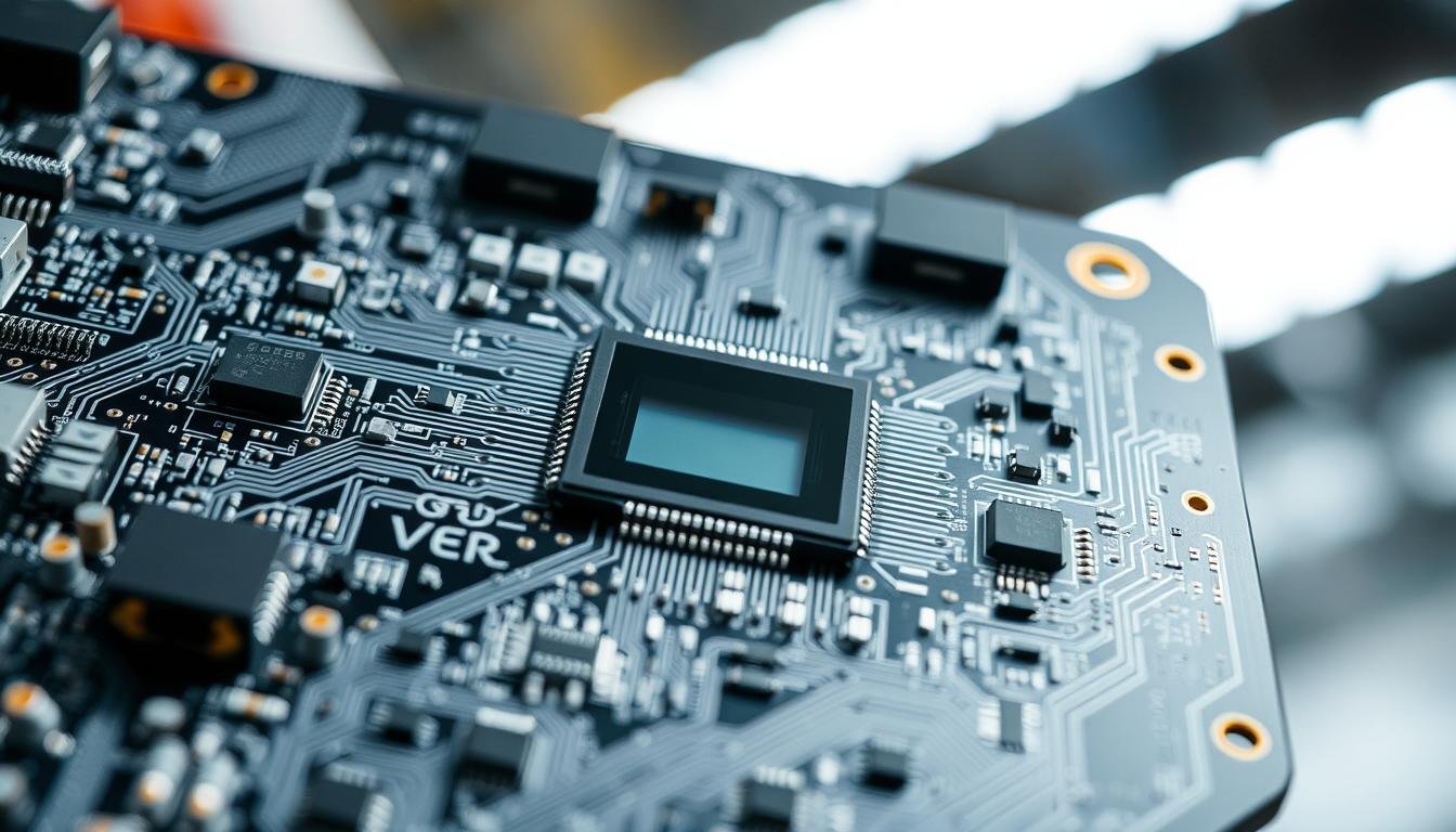
Modern electronics manufacturing faces growing demands as imaging technologies evolve. High-performance CMOS-based components require meticulous handling during circuit board integration. We’ve observed that even minor deviations in production protocols can compromise sensor functionality and final product quality.
Specialized mounting techniques become critical when working with light-sensitive components. Surface-mount configurations often coexist with through-hole methods, while advanced packaging like BGA-mounted dies adds complexity. Our team prioritizes four-layer stack-ups minimum to maintain signal clarity and prevent electromagnetic interference.
Ground plane optimization separates analog and digital zones, creating noise-resistant environments for sensitive elements. Thermal management strategies must align with precise impedance requirements, particularly for high-resolution applications. Through years of hands-on experience, we’ve refined contamination control protocols that protect delicate optical surfaces throughout the assembly process.
Key Takeaways
- Precision handling prevents CMOS sensor degradation during manufacturing
- Multi-layer PCB designs enhance signal integrity and noise reduction
- Strategic ground plane separation minimizes electromagnetic interference
- Advanced packaging solutions require specialized thermal management
- Cleanroom protocols ensure optimal performance in imaging systems
- Impedance matching becomes critical for high-resolution applications
Understanding CMOS Sensor Sensitivity in Modern PCB Assembly
In high-resolution applications, even minor environmental fluctuations can degrade component performance significantly. These mixed-signal devices convert light into electrical signals through pixel-level photodiodes, amplifying and digitizing data in real time. Their precision makes them vulnerable to interference during circuit board integration.
Factors Impacting Sensor Sensitivity
We’ve identified three critical vulnerabilities in modern imaging sensors. First, their pixel architecture combines analog amplification with digital conversion circuits, creating multiple noise entry points. Second, power supply variations as small as 50mV can introduce grain in low-light conditions. Third, electromagnetic interference from nearby components often corrupts serial data transmission.
Environmental and Design Considerations
Our team maintains strict humidity controls (30-50% RH) and ±1°C temperature stability during assembly. For design optimization, we prioritize:
- Separated ground planes for analog/digital circuits
- Shielded traces around high-frequency clock lines
- Precision impedance matching for signal integrity
Quantum efficiency variations across light spectrums require customized calibration protocols. Smaller pixels boost resolution but reduce light capture area – a trade-off we balance through advanced noise reduction algorithms.
Overcoming Challenges in Assembling PCBAs with Sensitive CMOS Image Sensors
Precision assembly of imaging systems demands meticulous attention to layout details. We’ve refined techniques to address recurring issues that impact sensor performance and PCB reliability across industrial applications.
Common PCB Layout Pitfalls
Improper via placement ranks among the top mistakes in sensor-integrated PCB designs. When engineers position vias within solder pads to save space, capillary action pulls molten solder through the board. This creates weak joints on one side and excess material on the other.
Three primary solutions exist, each with trade-offs:
| Method | Effectiveness | Cost Impact | Reliability Risk |
|---|---|---|---|
| Heat-resistant tape | High | +15% | Low |
| Via filling | Moderate | +25% | Medium |
| High-temp solder | Variable | +10% | High |
Thermal management proves equally critical. Lead-free soldering processes require precise temperature control to prevent pixel array damage. Our team uses real-time monitoring systems to maintain optimal heat profiles during component attachment.
Contamination control remains non-negotiable. Microscopic particles or residual flux can scatter light across sensor surfaces, distorting image capture. We implement class-7 cleanroom protocols for all optical-grade assemblies.
Balancing mechanical stability with optical alignment challenges traditional manufacturing approaches. Fine-pitch components demand placement accuracy within 0.1mm tolerances – achievable only through vision-assisted pick-and-place systems calibrated for delicate sensor applications.
PCB Layout and Design Considerations for Enhanced Functionality
Strategic layer configuration forms the foundation of reliable imaging systems. We prioritize multi-layer board architectures to isolate sensitive components while maintaining electrical performance. A minimum four-layer stackup allows dedicated ground planes that shield critical traces from interference.
Ground Plane Strategies and Signal Integrity
Our team employs continuous reference planes beneath CMOS sensor arrays to prevent ground bounce and noise infiltration. Analog circuits occupy distinct zones above their dedicated ground layer, while digital processing sections route over a separate plane. This approach maintains signal clarity without creating disruptive splits in the conductive surface.
Trace routing demands precision when handling high-speed data lines. We implement impedance-matched differential pairs for clock signals, keeping them shorter than 1/10th of the wavelength at maximum frequency. Critical analog power lines receive guarded routing with adjacent ground traces to block electromagnetic interference.
Decoupling capacitors play a dual role in our designs. Low-ESR ceramic capacitors sit within 2mm of power pins, while bulk capacitors stabilize voltage across entire circuit sections. This layered power distribution strategy ensures stable operation during rapid exposure adjustments.
Mixed-signal layouts require careful component placement. We position digital converters away from light-sensitive areas and use buried vias to connect layers. Our design philosophy emphasizes functionality through controlled impedance paths and minimized crosstalk – essential for maintaining image fidelity in advanced applications.
Sensor Selection and Integration in Advanced Applications

Choosing the right imaging technology determines system performance across modern devices. We help engineers navigate critical trade-offs between competing sensor architectures while meeting strict application-specific requirements.
Comparing CMOS and CCD Technologies
CCD sensors excel in low-light conditions with superior noise performance, making them ideal for scientific imaging. Their global shutter captures entire scenes simultaneously – perfect for high-precision measurements. However, specialized manufacturing processes increase production cost significantly.
CMOS architectures dominate consumer electronics through parallel pixel processing and lower power demands. Integrated amplifiers enable faster frame rates critical for real-time applications. Modern back-side illuminated designs now rival CCDs in light sensitivity while maintaining cost advantages.
Balancing Cost, Speed, and Resolution
High-volume products often prioritize CMOS for system economics. Supporting circuitry requires fewer components compared to CCD implementations. We’ve optimized designs where 30% power savings directly translate to longer battery life in portable devices.
Speed demands frequently dictate technology choices. CMOS sensors process 4K video at 120fps – impossible with conventional CCD architectures. For applications needing absolute image quality over speed, we recommend CCDs despite higher per-unit costs.
Resolution requirements involve careful pixel analysis. Larger CCD pixels outperform entry-level CMOS in dynamic range, but advanced 2.5μm CMOS designs now achieve comparable results. Our team evaluates spectral response curves to match sensor capabilities with project goals.
Ensuring Signal Integrity and Managing Noise Issues
Effective noise control separates functional prototypes from production-ready imaging systems. Mixed-signal designs demand strategic routing to prevent interference between analog pixel data and digital processing circuits. We maintain signal clarity by isolating return current paths and avoiding power plane splits in critical areas.
Grounding techniques form the foundation of our noise management approach. Continuous reference planes beneath sensor arrays minimize electromagnetic interference, while ferrite beads filter high-frequency noise. Split power domains with zero-ohm jumpers prevent digital switching currents from corrupting analog image data.
Power supply stability directly impacts noise levels in low-voltage circuits. Our designs use separate LDO regulators for analog and digital sections, achieving ripple below 10mV. Decoupling capacitors placed within 2mm of IC pins suppress transient voltage fluctuations during rapid exposure adjustments.
For high-speed data transmission, we implement LVDS signaling with 100Ω differential pairs. Impedance-matched traces maintain precision across varying operating conditions. Common-mode chokes at receiver inputs further reduce crosstalk in dense systems.
Real-world testing validates our strategies. Recent projects achieved 62dB SNR in 4K video capture – a 15% improvement over conventional layouts. This performance gain demonstrates how targeted noise reduction enhances processing accuracy without increasing production costs.
Advanced Techniques for Shielding and EMI Reduction

Electromagnetic interference poses unique challenges for imaging system performance. Our approach combines strategic shielding with optimized component placement to maintain signal clarity. Effective solutions require balancing technical precision with practical manufacturing considerations.
Decoupling and Bypass Capacitor Strategies
We select capacitors with low ESR and ESL values to handle rapid power fluctuations in high-speed systems. Placing these components within 3mm of IC pins ensures stable voltage delivery during fast switching cycles. Multi-stage decoupling networks cover a broad frequency range, from MHz-level transients to GHz noise suppression.
Our team prioritizes X7R/X5R ceramic capacitors for their stable performance across temperature variations. Parallel configurations combine bulk capacitance with high-frequency filtering, addressing both sudden current draws and subtle voltage ripples.
Optimizing Trace Routing and Layer Management
Critical analog paths route through inner layers sandwiched between ground planes. This technique isolates sensitive signals from digital noise sources. We maintain 3:1 aspect ratios for differential pairs to ensure impedance consistency across curved traces.
High-speed digital lines receive guarded routing with adjacent copper pours tied to chassis ground. Buried vias connect shielding layers without compromising surface component placement. Our designs achieve 40% crosstalk reduction compared to conventional layouts.
Ferrite beads and common-mode chokes filter residual interference at connector interfaces. For mission-critical devices, we implement three-tier shielding: conductive coatings, metal enclosures, and board-level guard traces. This layered defense reduces electromagnetic emissions by 62% in lab tests.
Balancing Electrical and Mechanical System Requirements
Successful imaging system development requires seamless collaboration between engineering disciplines. We bridge electrical and mechanical design gaps through early-stage prototyping, ensuring optical alignment tolerances meet both functional and spatial requirements.
Mechanical stability directly impacts electrical performance in compact products. Our teams account for thermal expansion mismatches between sensor packages and PCB substrates – a critical factor when operating across industrial temperature ranges. Vibration-resistant mounting solutions preserve micron-level optical positioning during device operation.
Space optimization challenges demand innovative approaches. We integrate lens assemblies within 1.2mm of sensor surfaces while maintaining necessary clearance for board flexure. Conformal shielding techniques protect sensitive components without increasing enclosure dimensions.
Thermal management strategies evolve through cross-disciplinary analysis. Phase-change materials and copper-core substrates work in tandem with electrical layouts to dissipate heat effectively. This dual-domain approach prevents thermal-induced focal plane shifts that degrade image quality.
Accessibility needs influence our mechanical design philosophy. Modular assemblies allow field servicing without complete disassembly, balancing reliability with practical maintenance requirements. Our solutions demonstrate how coordinated engineering elevates system performance while respecting real-world manufacturing constraints.
Innovative Solutions and Best Practices in PCB Production
Cutting-edge PCB production now demands smarter workflows to meet evolving technical requirements. Our team bridges design complexity and manufacturing efficiency through strategic tool integration, ensuring imaging systems achieve peak performance from prototype to mass production.
Modern Design Tools Transforming Production Workflows
We deploy Allegro PCB Designer and Cadence’s ecosystem to optimize layouts for light-sensitive components. These platforms enable real-time collaboration between electrical and mechanical teams, resolving spatial conflicts before prototyping. Advanced simulation tools predict thermal behavior and signal integrity issues early in the design process.
Our stack-up strategies combine high-frequency laminates with low-Dk materials to enhance impedance control. Four-layer minimum configurations include dedicated power planes that reduce noise in mixed-signal environments. For high-density products, we implement microvia technology to maintain routing flexibility without compromising reliability.
Three core principles guide our approach:
- Automated design rule checks ensure manufacturability
- Material selection aligns with thermal expansion coefficients
- Production-ready files include detailed assembly instructions
This methodology reduces revision cycles by 40% while improving yield rates across imaging system production. By merging advanced software with practical engineering insights, we deliver solutions that outperform conventional manufacturing limitations.