Can high-frequency applications be optimized without compromising signal integrity? As we explore the intricacies of RF and microwave circuit board designs, it becomes clear that these specialized PCBs require unique considerations to minimize interference and ensure optimal performance.
Unlike conventional circuit board designs, RF and microwave PCBAs demand precise control over parameters such as radio-frequency trace, power supply decoupling, via holes, and PCB stack-up. We will examine the critical factors that differentiate these high-frequency applications from their conventional counterparts.
Key Takeaways
- Understanding the unique challenges of high-frequency applications in RF and microwave PCBA design.
- The importance of material selection and stack-up configuration for optimal performance.
- Techniques for minimizing signal loss and reducing electromagnetic interference (EMI).
- Best practices for achieving reliable performance in telecommunications, radar systems, and wireless devices.
- Practical insights based on industry expertise to guide RF and microwave PCBA design.
Understanding the Unique Requirements of RF and Microwave PCBAs
Designing RF and microwave PCBAs requires a deep understanding of the unique challenges posed by high-frequency signals. Unlike conventional PCBs, RF and microwave designs must contend with factors that significantly impact signal integrity and overall performance.
How RF PCBs Differ from Conventional Designs
RF PCBs differ from conventional designs primarily in their need to manage high-frequency signal behavior. Signal integrity becomes a critical concern as frequencies increase, necessitating careful consideration of the PCB’s electrical properties. The dielectric constant of the material, for instance, plays a crucial role in determining signal propagation speed. Materials with a higher dielectric constant (Dk > 4) slow down signal propagation, potentially causing timing issues. Moreover, the geometry of traces and the overall stack-up design significantly impact impedance control, which is vital for maintaining signal quality.
Critical Parameters for High-Frequency Performance
Several critical parameters directly influence high-frequency performance in RF PCB designs. These include the dielectric constant (Dk), loss tangent, impedance control, and signal propagation velocity. Understanding how these parameters affect signal integrity is crucial for designing RF circuits that maintain signal quality across the intended frequency range. For instance, a higher loss tangent can lead to increased signal attenuation, while improper impedance matching can result in signal distortion. By carefully managing these factors, designers can ensure optimal performance in RF and microwave applications.
Controlled impedance, minimal signal reflections, and proper grounding form the foundation of successful RF design. By understanding and addressing these critical parameters, we can establish a framework for the detailed design considerations that follow in subsequent sections.
Material Selection for RF and Microwave PCBAs
Material selection is a critical step in the design of RF and microwave PCBAs, impacting both electrical performance and manufacturing processes. The choice of material affects signal propagation, attenuation, and overall system reliability.
Dielectric Properties and Their Impact on Signal Propagation
The dielectric properties of a material, including its dielectric constant (Dk) and dissipation factor (Df), play a crucial role in signal propagation. Materials with stable Dk values ensure consistent impedance, while low Df values minimize signal loss. PTFE (polytetrafluoroethylene) and ceramic-based materials are popular for their favorable dielectric properties.
Loss Tangent and Signal Attenuation Considerations
Loss tangent, another critical parameter, directly influences signal attenuation. Materials with low loss tangents are preferred for high-frequency applications to minimize signal loss. Rogers material, known for its low loss tangent, is a common choice for RF circuit boards, especially for 5G PCB designs.
Recommended Materials for Different Frequency Ranges
Different frequency ranges require specific materials. For lower RF frequencies (below 1 GHz), enhanced FR-4 materials may suffice. However, higher frequencies demand specialized materials like PTFE, ceramics, or hydrocarbon composites. We recommend considering materials from manufacturers like Rogers, Isola, Taconic, and Arlon, as they offer a range of options tailored to different applications.
When selecting materials, it’s essential to consider not only electrical performance but also manufacturing processes, reliability, and overall project costs. Hybrid material approaches, combining standard FR-4 with high-frequency laminates, can provide cost-effective solutions for mixed-signal designs.
- For lower RF frequencies, enhanced FR-4 materials can be used.
- Higher frequencies require specialized materials like PTFE or ceramics.
- Hybrid material approaches can offer cost-effective solutions.
Optimizing Stack-Up Design for RF Applications
The stack-up design of a PCB is a critical factor in RF circuit performance, affecting both signal propagation and thermal stability. We will explore the key considerations for optimizing stack-up design to meet the demanding requirements of RF applications.
Layer Sequencing and Isolation Best Practices
Proper layer sequencing is essential for minimizing crosstalk and ensuring isolation between sensitive RF signals. We recommend arranging RF signals and components on outer layers, while dedicating inner layers to ground and power planes. This configuration helps to reduce electromagnetic interference and improve overall signal integrity.
Maintaining Stack-Up Symmetry for Thermal Stability
Maintaining symmetry in the stack-up design is crucial for ensuring thermal stability. Asymmetric stack-ups can lead to warping or bending of the PCB, potentially causing mechanical stress on components. By balancing the layer configuration, we can minimize these risks and ensure reliable performance.
Determining Optimal Layer Count for RF Designs
Determining the optimal layer count is a critical aspect of RF PCB design. While 2-layer stack-ups may be sufficient for simple, low-frequency applications, most RF designs benefit from at least 4 layers to provide dedicated ground and power planes. For more complex designs, 6 to 12 layers are common, offering greater routing flexibility and improved isolation between critical signals.
When designing RF PCBAs, it’s essential to balance layer count with manufacturing complexity and cost. By understanding the trade-offs and optimizing the stack-up design, we can achieve the best possible performance for our RF applications.
Impedance Matching Techniques for Maximum Power Transfer
Effective impedance matching is critical in RF circuits to ensure that the maximum amount of power is transferred from the source to the load. Impedance matching is a crucial aspect of RF and microwave PCBA design, as it directly impacts the performance and efficiency of the circuit. We will explore the techniques used to achieve impedance matching, including understanding characteristic impedance, common impedance matching networks, and practical tips for achieving tight impedance tolerance.
Understanding Characteristic Impedance in RF Circuits
Characteristic impedance is a fundamental concept in RF circuit design, referring to the impedance that a transmission line would have if it were infinitely long. In RF PCBAs, maintaining a consistent characteristic impedance is vital to prevent signal reflections and ensure maximum power transfer. The characteristic impedance of a transmission line is determined by its physical properties, including the dielectric constant of the material, the trace width, and the thickness of the substrate. By understanding and controlling these factors, designers can achieve the desired characteristic impedance for their RF circuits.
Common Impedance Matching Networks (L, T, and Pi)
Impedance matching networks are used to match the impedance of different components or circuits in RF PCBAs. The most common types of impedance matching networks are L, T, and Pi configurations. These networks consist of combinations of inductors and capacitors that are designed to provide a specific impedance transformation. The choice of matching network depends on the specific application, frequency range, and desired impedance transformation. By using these networks, designers can achieve optimal impedance matching and maximize power transfer in their RF circuits.
Practical Tips for Achieving Tight Impedance Tolerance
Achieving tight impedance tolerance is essential for high-performance RF applications. While the standard industry tolerance for impedance control is typically ±10%, high-performance RF applications often require tighter tolerances of ±5% or better. To achieve this, designers can use simulation tools to model and analyze impedance characteristics, refining their designs iteratively to achieve optimal performance. Additionally, understanding the relationship between design parameters and manufacturing capabilities is crucial for specifying realistic impedance tolerances that can be reliably produced. By working closely with PCB fabricators and using advanced manufacturing techniques, designers can achieve the tight impedance tolerances required for their RF PCBAs.
To further optimize impedance matching, we recommend striving for tighter impedance tolerance, using simulation tools to model and analyze impedance characteristics, and understanding the impact of material selection, trace geometry, and manufacturing processes on impedance control. By following these practical tips and working with experienced PCB fabricators like Sierra Circuits, who offer tighter tolerances of ±5%, designers can achieve optimal impedance matching and maximize power transfer in their RF circuits.
RF Trace Design and Routing Strategies
RF trace design and routing strategies are critical components in the development of high-quality, high-frequency PCBAs. The performance of RF and microwave circuits heavily relies on the careful design and implementation of traces that connect various components.
Microstrip vs. Coplanar Waveguide Transmission Lines
When designing RF traces, engineers must choose between microstrip and coplanar waveguide (CPW) transmission lines. Microstrip lines are commonly used due to their simplicity and ease of fabrication. They consist of a conductor on one side of the substrate and a ground plane on the other. In contrast, coplanar waveguides have both the signal trace and ground planes on the same side of the substrate, offering better isolation and reduced radiation loss. The choice between these two depends on the specific application requirements and the frequency range of operation.
Trace Geometry Considerations for Signal Integrity
The geometry of RF traces significantly impacts signal integrity. Factors such as trace width, thickness, and the dielectric properties of the surrounding material all influence the characteristic impedance of the trace. Impedance matching is crucial to prevent signal reflections and ensure maximum power transfer. By carefully controlling trace geometry, designers can minimize signal attenuation and distortion, thereby maintaining signal integrity.
Mitering Techniques for RF Trace Corners
Sharp 90° corners in RF traces can cause impedance discontinuities and radiation, leading to signal reflections and EMI issues. To mitigate these effects, mitering techniques are employed. Mitering involves cutting away a portion of the trace corner to maintain a consistent impedance across the bend. The mitering width (M) can be calculated using the formula related to the trace width (W) and substrate height (H). By applying appropriate mitering techniques, designers can reduce signal reflections and maintain signal integrity, especially at high frequencies.
By understanding and applying these RF trace design and routing strategies, engineers can significantly enhance the performance and reliability of RF and microwave PCBAs.
Ground Plane Design Considerations for RF PCBAs

Ground plane design plays a pivotal role in RF PCBAs, influencing both the signal quality and the overall electromagnetic compatibility of the circuit. A well-designed ground plane is essential for providing a stable reference for signal voltages and currents, as well as for managing electromagnetic fields within the PCB.
Creating Effective Return Paths for RF Signals
To ensure optimal performance, it’s crucial to create effective return paths for RF signals. This involves designing a ground plane that offers low impedance to high-frequency currents. Ground vias are critical in this regard, as they provide a direct path to ground for RF signals, minimizing parasitic inductance and reducing the risk of electromagnetic interference. By liberally adding ground vias throughout the RF section, designers can significantly improve the PCB’s electromagnetic compatibility.
Via Placement Strategies for Minimizing Parasitic Inductance
Strategic via placement is key to minimizing parasitic inductance in RF designs. As frequencies rise, the importance of optimal via placement becomes increasingly critical. Via fencing or via stitching around RF traces and components is an effective technique for containing electromagnetic fields and preventing unwanted coupling between adjacent circuits. The diameter, spacing, and arrangement of vias all impact their parasitic inductance and current-carrying capacity. By understanding these factors, designers can determine the optimal via density and placement patterns for their specific application, thereby minimizing ground impedance throughout the design.
| Via Placement Strategy | Description | Benefits |
|---|---|---|
| Via Fencing | Placing vias around RF traces and components | Contains electromagnetic fields, reduces coupling |
| Via Stitching | Connecting ground planes on different layers with vias | Lowers impedance, improves electromagnetic compatibility |
| Ground Via Array | Array of vias providing multiple ground connections | Reduces parasitic inductance, improves signal integrity |
Component Selection and Placement for RF Circuits
Component selection and placement play a pivotal role in the functionality and efficiency of RF circuits. The performance of these circuits is significantly influenced by the choice and positioning of components. We need to carefully consider several factors to ensure optimal RF circuit performance.
Choosing RF-Compatible Components
Selecting components that are compatible with RF frequencies is crucial. We must consider the frequency-dependent behavior of components, including their parasitic elements. For instance, capacitors used in RF circuits must have suitable dielectric materials and constructions to minimize losses.
Strategic Component Placement to Minimize Interference
Strategic placement of components is vital to minimize electromagnetic interference (EMI) and ensure signal integrity. We should place sensitive components away from potential sources of interference and use grounding strategies effectively. The layout should also facilitate easy debugging and maintenance.
Decoupling Capacitor Placement in RF Designs
Effective power decoupling is critical in RF circuit designs. We achieve this by strategically placing decoupling capacitors to minimize the loop area between the capacitors, power pins, and ground connections. Using vias to connect decoupling capacitors directly to the ground plane can significantly reduce parasitic inductance.
By implementing multi-stage decoupling strategies with capacitors of different values, we can provide effective bypassing across wide frequency ranges. This approach ensures stable power delivery to RF circuits, enhancing overall performance and reliability.
Thermal Management in High-Frequency PCB Designs
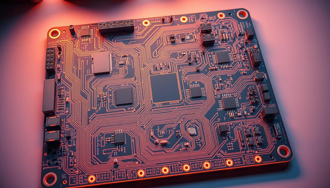
, showcasing its thermal management features. In the foreground, intricate copper traces and vias dissipate heat from the active components. The middle ground features a dense array of heat-sinking vias and thermal planes, strategically placed to efficiently transport thermal energy. In the background, a complex network of cooling fins and heatsinks, illuminated by warm, directional lighting, create an atmosphere of technical sophistication. The scene conveys the importance of comprehensive thermal management in the design of high-frequency, high-power PCBAs.")
Effective thermal management is crucial for the reliability and performance of high-frequency PCB designs. As we push the boundaries of RF applications, managing heat becomes increasingly critical to prevent degradation and ensure optimal functionality.
Heat Dissipation Challenges in RF Applications
High-frequency components and circuits generate significant heat due to high power densities. This heat must be efficiently dissipated to maintain the reliability of the PCB. Challenges arise from the compact nature of modern RF designs, where high power components are often closely packed, making it difficult to dissipate heat effectively.
Thermal Design Strategies for RF Components
To address these challenges, we employ several thermal design strategies. Thermal vias, copper coins, and embedded heat sinks can be used to create effective thermal paths from hot components to cooling surfaces. The choice of PCB material and copper thickness also plays a crucial role in thermal conductivity and heat spreading throughout the PCB. For more information on high-frequency RF board design, visit https://hilelectronic.com/high-frequency-rf-board-design/.
Advanced cooling techniques, including interface materials, mechanical heat sinks, and active cooling systems, are considered when passive approaches are insufficient for high-power RF applications. Balancing electrical performance with thermal requirements is key to successful thermal management.
Manufacturing Considerations for Hybrid RF PCBs
Hybrid RF PCB manufacturing is a complex process that necessitates a deep understanding of material properties and fabrication techniques. To achieve high-quality RF PCBs, designers must consider several critical factors, including the coefficient of thermal expansion (CTE) differences between materials, the consistency of plated through-holes, and the capabilities of PCB fabricators.
Managing CTE Differences
Managing CTE differences is crucial because RF PCBs often combine materials with varying thermal expansion properties. For instance, Rogers 5880, a popular RF material, contracts after copper etching, requiring fabricators to compensate for this shrinkage. Ensuring that all materials work harmoniously together is key to maintaining the structural integrity and performance of the PCB.
Plated Through-Hole Consistency Challenges
Plated through-holes (PTHs) are critical for the reliability of RF PCBs, but achieving consistency can be challenging due to the varying densities and properties of the materials used. Fabricators must employ precise techniques to ensure that PTHs are consistent and reliable, directly impacting the overall quality of the PCB.
Working with PCB Fabricators for RF Designs
Collaborating with experienced PCB fabricators early in the design process is essential for successful RF PCB manufacturing. Fabricators can provide valuable insights into material compatibility and manufacturing constraints, helping designers create PCBs that meet both performance and manufacturability requirements. We guide designers in selecting the right fabricators and developing comprehensive fabrication documentation that ensures their RF designs are executed with high quality.
By understanding the manufacturing process and working closely with fabricators, designers can ensure that their hybrid RF PCBs are both high-performance and manufacturable. This collaboration is key to avoiding costly redesigns and achieving the desired quality in the final product.
Conclusion: Ensuring Successful RF and Microwave PCBA Designs
In conclusion, the design of RF and microwave PCBAs necessitates a deep understanding of high-frequency signal propagation and its impact on the design process. We’ve explored the critical design considerations that differentiate RF and microwave PCBAs from conventional circuit boards, providing a comprehensive framework for successful high-frequency design.
By integrating material selection, stack-up configuration, impedance control, and thermal management into a cohesive strategy, designers can create RF and microwave PCBs that deliver optimal performance and reliability. Remember, RF design is both a science and an art, requiring experience and continuous learning to master the complexities of high-frequency circuit design.