In the realm of high-speed PCB design, signal integrity and manufacturability often seem to be competing priorities. Engineers focus on maintaining clean signals while manufacturers emphasize production efficiency. Design for Manufacturability (DFM) for Signal Integrity bridges this gap, ensuring that high-performance designs can be reliably manufactured at scale. This comprehensive guide explores how proper DFM practices not only improve manufacturing yields but also enhance signal integrity in high-speed PCB assemblies.
Why DFM Matters for Signal Integrity
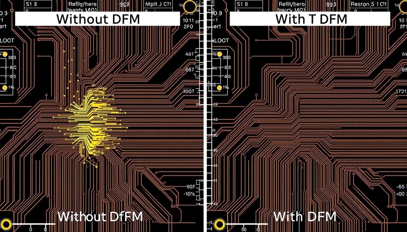
Figure 1: Signal quality comparison between designs with and without DFM considerations
Signal integrity refers to a signal’s ability to carry information reliably while resisting degradation from noise, distortion, and timing issues. As data rates increase beyond 10 Gbps, even minor manufacturing variations can significantly impact signal quality. DFM practices ensure that design specifications translate accurately to physical boards, maintaining critical parameters like impedance control, crosstalk mitigation, and timing requirements.
The relationship between manufacturing processes and signal integrity is often underestimated. Manufacturing variations in trace width, dielectric thickness, copper roughness, and via structures directly affect impedance, propagation delay, and signal loss. By implementing DFM for signal integrity, designers can create robust designs that maintain performance despite normal manufacturing tolerances.
Signal integrity issues that appear during testing often originate from DFM oversights rather than fundamental design flaws. Addressing these issues early in the design phase is significantly more cost-effective than resolving them after manufacturing.
Key Signal Integrity Challenges in High-Speed PCBAs
Before diving into best practices, it’s essential to understand the primary signal integrity challenges that proper DFM can address:
Impedance Control Issues
Maintaining consistent impedance throughout signal paths is critical for high-speed designs. Manufacturing variations in trace width, height, and dielectric constant can cause impedance fluctuations that lead to reflections and signal degradation.

Figure 2: Impedance discontinuities caused by manufacturing variations
Via-Related Signal Degradation
Vias introduce impedance discontinuities, parasitic capacitance, and inductance that can degrade signals. Via stubs (unused portions of plated through-holes) create resonant structures that cause frequency-dependent signal loss, particularly problematic above 10 Gbps.

Figure 3: Via structures and their impact on signal paths
Crosstalk and EMI
As component density increases and trace spacing decreases, crosstalk between adjacent signals becomes more pronounced. Manufacturing variations in spacing and layer registration can exacerbate crosstalk issues, while improper grounding structures can increase electromagnetic interference (EMI).

Figure 4: Crosstalk coupling mechanisms between adjacent traces
Material and Process Variations
PCB material properties, particularly dielectric constant and loss tangent, can vary between material batches and after manufacturing processes like lamination. These variations affect signal propagation speed and loss, potentially causing timing issues and signal attenuation.

Figure 5: Impact of dielectric constant variations on signal propagation
Identify Signal Integrity Issues Before Manufacturing
Our comprehensive DFM for Signal Integrity Checklist helps you identify and resolve potential issues before they impact your high-speed designs.
Material Selection for Signal Integrity
The foundation of signal integrity begins with proper material selection. High-speed designs require materials with specific electrical properties and consistent manufacturing characteristics.
Low-Loss Laminates

Figure 6: Comparison of laminate materials for high-speed applications
Standard FR-4 materials often prove inadequate for designs operating above 10 Gbps due to their relatively high loss tangent and dielectric constant variation. Low-loss laminates specifically engineered for high-speed applications offer significant advantages:
| Material Type | Dk (Dielectric Constant) | Df (Loss Tangent) | Dk Tolerance | Suitable Data Rates | Relative Cost |
| Standard FR-4 | 4.0-4.5 | 0.020-0.025 | ±10% | Up to 5 Gbps | Low |
| Mid-Loss FR-4 | 3.8-4.2 | 0.015-0.018 | ±7% | 5-10 Gbps | Medium |
| Megtron 6 | 3.4-3.6 | 0.004-0.008 | ±5% | 10-25+ Gbps | High |
| Rogers RO4350B | 3.48 | 0.0037 | ±3% | 25-56+ Gbps | Very High |
DFM Considerations for Material Selection
Hybrid Stack-ups
To balance cost and performance, consider hybrid stack-ups that use high-performance materials only for critical signal layers. When implementing hybrid stack-ups, ensure your manufacturer has experience with these constructions, as they require special processing to prevent delamination and warping.

Figure 7: Hybrid stack-up using different materials for optimal performance/cost balance
Material Consistency
Ensure your manufacturer can maintain material consistency across production runs. Specify that all boards within a production lot use materials from the same batch to minimize variations in dielectric constant and loss tangent. This consistency is particularly important for impedance-controlled designs.
Trace Routing Strategies for Signal Integrity
Proper trace routing is essential for maintaining signal integrity in high-speed designs. DFM considerations must be incorporated into routing strategies to ensure manufacturability without compromising performance.
Controlled Impedance Design

Figure 8: Controlled impedance structures with manufacturing tolerance bands
Controlled impedance is critical for high-speed signal integrity. When designing for manufacturability, consider these key factors:
Trace Width and Spacing
Design trace widths that can be reliably manufactured. For high-speed signals, maintain a minimum trace width of 5 mils (0.127mm) for outer layers and 4 mils (0.102mm) for inner layers. This ensures consistent copper etching and reduces impedance variations.
For differential pairs, maintain consistent spacing throughout the route. Specify spacing based on the manufacturer’s capabilities, typically no less than 5 mils (0.127mm) for standard processes. Tighter spacing may be possible with advanced manufacturing but will increase cost.
Manufacturing Tolerances
Account for manufacturing tolerances in impedance calculations. Typical manufacturing processes can maintain trace width within ±0.5 mil (0.0127mm) and dielectric height within ±10%. Design impedance targets with these tolerances in mind.
DFM Tip: For critical high-speed signals (25+ Gbps), specify tighter impedance control (±5% rather than standard ±10%) and work with manufacturers who can verify impedance through TDR testing.
Calculate Precise Impedance Values
Our online Impedance Calculator helps you determine the exact trace dimensions needed for your target impedance, accounting for manufacturing tolerances.
Length Matching and Skew Control

Figure 9: Length matching techniques for differential pairs
Length matching is essential for maintaining signal timing relationships. From a DFM perspective, consider these practices:
Serpentine Routing
When implementing serpentine traces for length matching, maintain minimum bend radius (typically 3x trace width) to avoid impedance discontinuities. Space serpentine segments at least 3x trace width apart to minimize coupling between segments.
Manufacturing-Friendly Length Matching
Specify length matching requirements based on signal speed and timing budgets. For differential pairs at 10 Gbps, maintain intra-pair skew below 5 mils (0.127mm). For 25+ Gbps, reduce this to 2 mils (0.051mm) or less.
Maximum allowable skew can be calculated as: Skew(max) = 0.1 × Rise Time. For a 25 Gbps signal with 14ps rise time, maximum skew should be under 1.4ps (approximately 1 mil or 0.0254mm in FR-4).
Via Optimization for Signal Integrity
Vias are often the most significant source of signal integrity issues in high-speed designs. Proper DFM for vias ensures reliable manufacturing while minimizing their impact on signal quality.

Figure 10: Comparison of via structures for high-speed applications
Via Stub Reduction
Via stubs create resonant structures that cause frequency-dependent signal loss. For signals above 10 Gbps, via stub reduction becomes critical:
Back-drilling
Back-drilling removes unused portions of via barrels, significantly reducing stub effects. From a DFM perspective, specify back-drill depth to leave no more than 10 mils (0.254mm) of stub for signals operating at 10-25 Gbps, and 5 mils (0.127mm) or less for signals above 25 Gbps.
When specifying back-drilling, account for drill depth tolerance (typically ±3 mils or 0.076mm). Specify the maximum allowable remaining stub rather than an exact drill depth.
Blind and Buried Vias
Blind and buried vias eliminate stubs entirely but increase manufacturing complexity and cost. For critical signals above 25 Gbps, the performance benefits often justify the additional cost. Ensure your manufacturer has experience with these structures and can reliably produce them.

Figure 11: Manufacturing process for blind and buried vias
Via Design for Manufacturability
Aspect Ratio
The aspect ratio (board thickness to hole diameter) is critical for reliable via plating. For standard through-hole vias, maintain aspect ratios below 10:1. For microvias, keep aspect ratios below 0.8:1 for reliable formation.
| Via Type | Maximum Aspect Ratio | Minimum Drill Size | Plating Challenges |
| Through-hole | 10:1 | 8 mil (0.2mm) | Uniform plating through entire barrel |
| Blind Via | 0.8:1 | 4 mil (0.1mm) | Consistent depth control |
| Buried Via | 8:1 | 8 mil (0.2mm) | Registration between layers |
| Microvia | 0.8:1 | 3 mil (0.075mm) | Consistent formation and filling |
Annular Ring
The annular ring (copper pad surrounding the drill hole) must be sufficient to accommodate drill registration tolerance. For high-speed signals, minimize annular rings to reduce parasitic capacitance while maintaining manufacturability.

Figure 12: Optimized annular ring design with teardrops
For high-speed signals (10+ Gbps), specify annular rings of drill diameter plus 8 mils (0.203mm) rather than the standard plus 10-12 mils. Add teardrops to maintain reliability with these reduced annular rings.
Expert Signal Integrity Consultation
Our signal integrity experts can review your high-speed designs and provide specific recommendations to optimize both performance and manufacturability.
EMI Mitigation Techniques
Electromagnetic interference (EMI) can significantly impact signal integrity in high-speed designs. Proper DFM practices for EMI mitigation ensure that grounding and shielding structures can be reliably manufactured.

Figure 13: EMI mitigation techniques for high-speed PCB designs
Ground Plane Design
Continuous Ground Planes
Maintain continuous, uninterrupted ground planes adjacent to signal layers. From a DFM perspective, specify minimum copper pour requirements (typically 70% minimum copper coverage) and avoid large cutouts or splits in ground planes.

Figure 14: Proper vs. improper ground plane implementations
Via Stitching
Via stitching connects ground planes across layers, reducing EMI and providing low-impedance return paths. For manufacturability, use standard-sized vias (minimum 8 mil or 0.2mm drill) spaced no more than λ/20 apart at the highest frequency of concern.
Stackup Design for EMI Control

Figure 15: Optimized stackup designs for signal integrity and EMI control
Proper stackup design is critical for both signal integrity and EMI control. From a DFM perspective, consider these key factors:
Layer Pairing
Pair signal layers with adjacent ground planes to provide tight field coupling and low-impedance return paths. Ensure your manufacturer can maintain tight layer-to-layer registration (typically ±2 mils or 0.051mm) to preserve this coupling.
The most effective stackup designs for high-speed signals use a “signal-ground-signal-ground” pattern that provides each signal layer with its own adjacent reference plane.
Symmetrical Construction
Design stackups with symmetrical construction around the center to prevent warping during manufacturing. This is particularly important for high-layer-count boards and those using mixed materials.
Specify core and prepreg thicknesses that your manufacturer can reliably produce. Standard thicknesses (e.g., 5 mil/0.127mm cores) are more consistent than custom thicknesses and typically result in better impedance control.
Case Study: DFM Improvements for a 28 Gbps Design

Figure 16: Before and after DFM improvements for a 28 Gbps design
A telecommunications equipment manufacturer was experiencing intermittent signal integrity issues with their 28 Gbps backplane design. Despite careful simulation during design, manufactured boards showed excessive jitter and eye closure that varied significantly between production lots.
Initial Challenges
DFM Improvements Implemented
Via Optimization
Back-drilling was implemented to reduce stub lengths to less than 5 mils (0.127mm). Annular rings were reduced from drill+12 mils to drill+8 mils with teardrops added for manufacturing reliability. These changes reduced parasitic capacitance and eliminated resonant frequency dips.
Material and Impedance Control
Material specifications were tightened to require consistent Dk (±3%) across production lots. Impedance tolerance was reduced from ±10% to ±5% with additional test coupons added to each panel for verification. Trace width tolerances were tightened from ±1 mil to ±0.5 mil.
Results
The DFM improvements resulted in significantly better signal integrity performance and more consistent results across production lots. Eye height increased by 90%, and jitter was reduced by 85%. Manufacturing yields improved from 76% to 98%, resulting in substantial cost savings despite the more stringent manufacturing requirements.
Conclusion: Integrating DFM into Signal Integrity Design

Figure 17: Integrated DFM and signal integrity workflow
Successful high-speed PCB design requires integrating DFM considerations throughout the signal integrity design process. By addressing manufacturability early in the design cycle, engineers can create designs that not only perform well in simulation but also maintain their performance when manufactured at scale.
Key takeaways for implementing DFM for signal integrity include:
By following these best practices, designers can create high-speed PCB designs that maintain signal integrity while achieving high manufacturing yields and consistent performance across production lots.
Master Signal Integrity in Your High-Speed Designs
Join our upcoming webinar to learn advanced techniques for maintaining signal integrity in high-speed PCB designs while ensuring manufacturability.