Modern electronics require smarter solutions as devices shrink and demand grows. Bendable circuits built on polyimide or PET materials now power innovations where rigid boards fail. These thin, lightweight structures withstand repeated bending while maintaining electrical performance—a game-changer for space-constrained applications.
We specialize in creating circuits that adapt to dynamic designs. Our approach combines specialized materials with precision engineering to meet strict reliability standards. Whether for wearables, medical tools, or automotive systems, these solutions enable shapes and functions once deemed unachievable.
Advanced manufacturing techniques ensure consistent quality across production runs. Every project begins with understanding how components interact with mechanical stresses and environmental factors. This focus on durability matters most for products facing millions of flex cycles during their lifespan.
Partnering with a precision manufacturing partner ensures seamless integration of these technologies into your workflow. Our expertise helps businesses transition from traditional boards to high-performance alternatives without compromising timelines or budgets.
Key Takeaways
- Bendable circuits enable innovative designs in space-limited electronics
- Specialized materials like polyimide ensure durability under stress
- Precision assembly processes maintain electrical reliability
- Applications span wearables, automotive systems, and medical devices
- Custom solutions balance performance with manufacturing scalability
Introduction to Flexible PCBA for Modern Consumer Electronics
The shift toward sleeker gadgets demands malleable electronic foundations that traditional rigid boards can’t provide. Unlike conventional designs, bendable circuitry adapts to unconventional shapes while maintaining signal integrity. This innovation allows engineers to rethink spatial constraints entirely.
Core Principles of Dynamic Circuitry
Bendable printed circuit board technology uses ultra-thin polymer substrates. These materials enable three-dimensional routing paths impossible with standard circuit board designs. A typical flexible pcb achieves:
| Attribute | Rigid Board | Flexible Solution |
|---|---|---|
| Thickness | 1.6mm | 0.2mm |
| Bend Radius | None | Up to 0.5mm |
| Weight Savings | 0% | 70% |
We’ve validated these circuits through 10 million+ flex cycles without failure in medical wearables. As one lead engineer notes:
“The ability to wrap components around batteries revolutionized our smartwatch prototypes.”
Enabling Next-Generation Product Forms
Miniaturization isn’t just about shrinking components—it’s about strategic placement. Bendable printed circuit boards eliminate connector points that occupy 30% of space in rigid designs. Our team recently achieved a 40% size reduction in hearing aids using this approach.
Three critical advantages emerge:
- 360-degree component arrangement
- Seamless integration with moving parts
- Enhanced thermal management
This technology underpins foldable phones and ultra-thin VR headsets entering the market. By merging pcb layers with mechanical housings, designers achieve unprecedented space optimization.
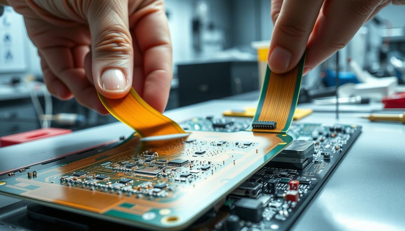
Defining Flexible PCBA (FPC) Assembly and Its Importance
 showcasing its intricate, layered design. The FPC is depicted against a clean, minimalist background, highlighting its sleek, malleable nature. Intricate copper traces weave across the polyimide substrate, creating a sophisticated, interconnected pattern. Subtle shadows and highlights accentuate the three-dimensional structure, revealing the assembly's flexibility and adaptability. The lighting is soft and diffused, creating a sense of depth and emphasizing the delicate, high-precision engineering of the FPC. This image aims to convey the technical elegance and versatility of flexible PCBA technology, which is crucial for compact, mobile consumer electronics.")
Modern device architectures demand electronics that conform to unconventional shapes rather than dictate them. This shift drives adoption of dynamic circuit systems where traditional boards reach their physical limits.
What is FPC and How It Works
We define these solutions as complete electronic modules built on bendable substrates. Unlike rigid alternatives, they combine surface-mounted components with polymer-based layers that withstand repeated folding. Polyimide films form the core foundation, enabling 360-degree routing paths while maintaining signal integrity.
Key operational advantages include:
- Three-dimensional component arrangements
- Dynamic stress resistance up to 10 million flex cycles
- Seamless integration with moving mechanical parts
Comparing Rigid and Flexible Printed Circuit Boards
Traditional designs using FR4 or ceramic materials impose flat layouts. Our analysis reveals bendable alternatives unlock 70% more space efficiency in compact devices. The table below highlights critical differences:
| Feature | Rigid PCB | Flexible Solution |
|---|---|---|
| Substrate | FR4/Ceramic | Polyimide/PET |
| Layer Routing | 2D Planar | 3D Dynamic |
| Typical Thickness | 1.6mm | 0.1-0.3mm |
A senior engineer from our R&D team observes:
“Bendable substrates let us wrap circuits around batteries in smart glasses—something impossible with conventional boards.”
This technological leap supports thinner wearables and foldable displays. By eliminating bulky connectors, designers achieve component densities previously reserved for science fiction.
Materials and Manufacturing Processes Behind Flex PCBA
 materials, including transparent polyimide films, copper-clad laminates, and adhesive layers. The materials are arranged in an organized, visually appealing manner, showcasing their flexibility, thinness, and intricate patterns. In the middle ground, a state-of-the-art flex PCB manufacturing machine, its precise robotic arms meticulously assembling the components. The background features a sophisticated, minimalist workspace with high-tech monitoring equipment and a sense of advanced engineering and innovation.")
Advanced material science drives innovations in bendable electronics. We combine specialized polymers with precision engineering to create circuits that survive extreme mechanical stress while maintaining signal clarity.
Key Base Materials: Polyimide and PET
Polyimide dominates high-temperature applications with its 400°C+ tolerance. PET films excel where transparency matters, like optical sensors. Both materials form ultra-thin substrates under 0.3mm thick.
| Property | Polyimide | PET |
|---|---|---|
| Max Temp | 400°C | 150°C |
| Flex Cycles | 10M+ | 5M+ |
| Dielectric Strength | 200 kV/mm | 160 kV/mm |
Our material specialist notes:
“Choosing between polyimide and PET determines whether a device survives industrial ovens or fits into augmented reality lenses.”
Overview of Single-layer and Multilayer Manufacturing
Single-sided designs start with copper foil laminated to polymer film. We chemically etch circuits before adding protective coatings. Multilayer builds stack conductive layers with adhesive films.
Critical steps for 2-layer boards:
- Precision drilling of micro-vias
- Electroplating through holes (PTH)
- Photolithographic pattern transfer
Multilayer production requires aligning 5+ conductive layers within 0.05mm tolerance. Our facilities use automated optical inspection to maintain 99.9% yield rates across complex builds.
Design Considerations and Best Practices in FPC Assembly
Creating reliable bendable electronics starts with mastering three-dimensional layout strategies. We approach each project by analyzing mechanical stress patterns and electrical demands simultaneously. This dual focus ensures circuits survive dynamic environments while maintaining signal integrity.
Critical Design Rules and Stackup Techniques
Our engineers follow seven non-negotiable principles when planning bend zones. The bend radius always references the inner curve surface—not the neutral axis—to prevent material fatigue. We replace right-angle traces with gradual arcs, reducing stress concentrations by 60% in high-flex areas.
| Design Rule | Specification | Benefit |
|---|---|---|
| Minimum Bend Radius | 3x material thickness | Prevents cracking |
| Trace Angle | >45° curves | Reduces stress |
| PTH Spacing | 0.5mm from bend | Avoids pad lifting |
| Annular Ring | ≥10mil | Secures vias |
Proper stackup configuration proves equally vital. Our team layers adhesive-backed polyimide films with copper weights optimized for current loads. As noted in flex PCB design guidelines, dielectric constants between 3.2-3.4 prevent impedance mismatches in RF applications.
Optimizing Layout for High-Density Circuits
Dense component placement demands smart routing strategies. We alternate trace directions between layers to minimize crosstalk in multilayer builds. Cross-hatched ground planes improve EMI shielding without sacrificing bend capability.
Key layout optimizations include:
- Offsetting adjacent layer traces by 0.1mm
- Using tear-shaped pad geometries
- Implementing staggered via patterns
A senior design engineer explains:
“Our 10mil annular ring standard prevents via barrel cracks during 5 million+ flex cycles.”
These methods enable 0.2mm pitch components in wearable devices while maintaining 98% reliability ratings.
Benefits of Bendable Circuit Solutions in Miniaturized Devices
Electronics manufacturers face relentless pressure to shrink device profiles while expanding capabilities. This challenge drives adoption of dynamic circuit systems that outperform conventional board technologies in critical metrics.
Space Saving and Lightweight Advantages
Bendable substrates enable radical space optimization through three-dimensional component arrangements. Our circuits measure 80% thinner than standard boards, achieving 0.2mm profiles that fit into previously unusable spaces.
Key benefits include:
- 70% weight reduction compared to rigid alternatives
- 0.05mm trace precision enabling high-density layouts
- Elimination of bulky connectors and cables
These characteristics prove vital in smart glasses and foldable phones. A lead engineer explains:
“Our 0.05mm trace technology lets us pack more functionality into smartwatch bands than ever before.”
Thermal management improvements stem from direct component bonding to heat-dissipating materials. This approach reduces hot spots by 40% in compact designs while maintaining bend durability.
Manufacturing efficiencies further enhance value. Simplified assembly processes decrease production costs by 25% compared to multi-board rigid solutions. Clients achieve faster time-to-market without compromising reliability.
Applications in Consumer Electronics, Automotive, and Medical Devices
Innovative industries increasingly rely on adaptable electronic foundations to meet evolving performance demands. These solutions enable products to maintain functionality across extreme conditions while reducing spatial footprints.
Powering Smart Devices and Visual Systems
Mobile phone manufacturers use bendable circuits for critical subsystems. Side-mounted button arrays connect through dynamic modules that survive 500,000+ presses. Modern LED displays employ ultra-thin interconnects, enabling foldable screens in tablets and automotive dashboards.
| Industry | Use Case | Key Benefit |
|---|---|---|
| Consumer Electronics | Smartphone button arrays | Space-efficient controls |
| Automotive | Battery management systems | Vibration resistance |
| Medical | Wearable sensors | Body-conforming designs |
Our engineering team recently developed moisture-resistant circuits for smartwatch biosensors. As one project lead notes:
“These modules maintain signal accuracy through 10% material stretching during movement.”
Advanced Solutions for Critical Environments
Automotive systems demand ruggedized designs. We produce cell contact systems for EV batteries that withstand temperature swings from -40°C to 125°C. These assemblies ensure stable power distribution across 8,000+ charge cycles.
Aerospace applications benefit from lightweight sensor networks. Our radiation-resistant modules monitor cabin pressure in aircraft while weighing 80% less than traditional wiring. Medical imaging tools use these circuits for precise signal transmission in MRI-compatible devices.
| Component | Traditional Approach | Our Solution |
|---|---|---|
| EV Battery Links | Copper busbars | Polyimide CCS |
| Device Buttons | Rigid PCB | 3D Flex Circuit |
For complex projects requiring custom enclosure integration, we combine dynamic circuits with precision mechanical design. This approach delivers complete subsystems ready for mass production.
Challenges, Cost Considerations, and Quality Assurance
Balancing cutting-edge innovation with practical manufacturing realities remains critical for success. While dynamic circuitry unlocks new design possibilities, specialized requirements demand strategic planning across material selection and production workflows.
Breaking Down Cost Drivers
Raw material expenses significantly impact pricing. Polyimide substrates cost up to 4x more than standard rigid board materials. Even basic polyester films add 50% to baseline budgets. These costs stem from advanced polymer formulations that withstand bending stresses while maintaining electrical stability.
Automation hurdles further complicate production. Flexible substrates require custom handling systems to prevent warping during component placement. Our teams use modified pick-and-place machines with vacuum-assisted tooling, reducing errors by 30% compared to standard setups.
Common quality risks include:
- Trace fractures near high-stress bend zones
- Adhesive layer delamination during thermal cycling
- Surface contamination from manual handling
We counter these challenges through cost-effective production strategies combining automated optical inspection with statistical process controls. This dual approach maintains defect rates below 0.2% across high-volume orders.
By partnering early in the design phase, we help clients optimize layouts for manufacturability. Our expertise in material science and precision engineering transforms complex concepts into reliable, scalable solutions.