Why is DFM Essential for PCB Production?
- Errors can occur in PCB design or during file format conversions. Our engineers meticulously check for these errors to ensure accuracy.
- The materials or technologies used in PCB designs might not be available with all manufacturers. We can recommend suitable alternatives to meet your design needs.
- We optimize aspects such as stack-up and material choices to enhance PCB robustness and cost-effectiveness.

Get a free quote now!
DFM Services at ESPCBA
At ESPCBA, our experienced engineers thoroughly inspect all your files, including Gerber files and design notes. Below are the key areas we assess:
Materials
If the specified material has a long lead time or is unavailable, we suggest alternatives and get customer approval. To lower costs and improve material utilization, we optimize the array layout, achieving at least 85% utilization for single/double-sided boards and 75% for multi-layer boards.
Drilling
We verify hole sizes and tolerances to ensure they fall within a reasonable range, addressing specific requirements like press-fit holes. A maximum tolerance of 2 mils is maintained for better assembly performance.
For small vias, solder mask ink can clog them, so plug holes are recommended. Larger vias can be downsized for improved results. We ensure proper via placement, especially near BGAs, to prevent issues like short circuits during SMT.
Buried-blind holes are essential for high-density multi-layer boards. By adjusting dielectric thickness, we achieve interconnection through any layer to meet buried-blind hole requirements.
Depth Control Drilling
This reduces technical difficulty and cost by removing unneeded sections of through-holes, improving signal transmission.
This ensures precise drilling depth for advanced PCB designs.
Copper Plating
We maintain uniform copper plating by adding auxiliary copper sheets. Data monitoring ensures electroplating parameters are optimal, and copper thickness is verified post-plating to ensure it meets design specifications.
Layup
We review lamination processes to avoid issues like delamination, especially for thick copper plates. For blind holes, we recommend suitable materials to prevent delamination during SMT. If needed, we adjust the design to meet thickness and impedance values.
CAM Design
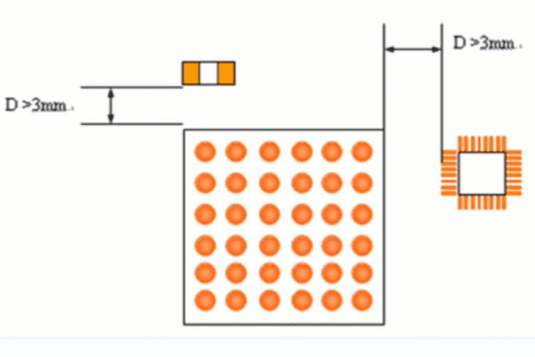
To optimize repairability, we suggest leaving a 3mm space around BGAs. For improved power filtering, placing capacitors near the BGA is recommended. We also refine via placement to enhance layout efficiency and signal integrity.
Using Polar software, we simulate impedance values and provide a detailed analysis report.
We recommend suitable panel types (V-cut or mouse bite) for efficient manufacturing and assembly. Adjustments to V-score designs help prevent copper exposure and ensure precision during PCB assembly.

Copper Layer Design
We follow key rules for copper layer design, ensuring clearances meet manufacturing requirements. Adjustments to pads, copper pours, and lines are made to maintain minimum gaps and meet etching tolerances.
IC Pin and Circuit Optimization
Lines connected to IC pins are adjusted for width and clearance to ensure manufacturability. Non-functional circuits are removed to avoid issues like peeling during fabrication.
Edge Copper Rules
We ensure adequate spacing between copper layers and board edges during routing and scoring. Tooling holes and fiducial marks are added to aid in alignment and prevent etching issues.
Drill Guidelines
For NPTH (Non-Plated Through Holes), the isolation clearance between the first drilled hole and the outer copper layer should generally be ≥ 0.20mm, with a minimum clearance of ≥ 0.15mm. This helps prevent issues like the silk screen line’s solder resistance from reddening.
- Second Drill Copper Removal: If the second drill occurs after etching, the copper cut should be 0.10mm smaller than the hole’s diameter on one side. If the second drill happens before routing, the minimum clearance from the edge of the drill to the copper or trace should be 0.10mm.
- Ensure the second drilled annular ring has a minimum of 0.3mm on one side after etching, especially for 2oz copper. A minimum ring of 0.3mm should be maintained on both sides.
Solder Mask Design
- Gerber File Check: Ensure solder mask files avoid covering pads.
- Solder masks should be exposed enough to minimize substrate leakage. The opening should be 1 mil larger than the pad on each side.
- For solder mask dams near golden fingers, we recommend removing them to expose the slot's ends if deemed unreasonable.
- BGA Design: For small BGA, poor etching control can be a concern, so choosing a solder mask defined by the pad is advisable.
- Vias around the BGA should be plugged with solder mask ink to reduce the risk of open or short circuits.
Solder Mask for PTH and NPTH
Holes ≤ 0.5mm should not be blocked by the solder mask. For holes larger than the opening but smaller than the pad, avoid ink entering the hole by using a solder mask blocking point that’s 0.1mm larger than the hole.
For NPTH holes ≥ 0.6mm, make the blocking point 0.05mm smaller than the hole's diameter. For holes < 0.6mm, make the blocking point 0.05mm larger than the hole's diameter. Cancel solder mask blocking points for plugged holes.
Film Design Principles
The window size and distance from the line are crucial. For different copper thicknesses, adjust the S/M opening size:
- For copper < 1oz: S/M opening should be 0.05mm larger than the pad on one side, typically 0.08mm.
- For 1oz ≤ copper < 2oz: S/M exposure should be 0.05mm larger than the compensated line or pad.
- For 2oz ≤ copper < 3oz: Increase the opening by 0.03mm.
- For 3oz ≤ copper < 4oz: Increase the opening by 0.02mm.
- For copper ≥ 4oz: S/M exposure should be 0.01mm larger than the pad or compensated line.
For BGA, the minimum S/M exposure should be 0.03mm larger than the pad or line for better exposure control.
Carbon Design
- Printing Pad: The printing pad should be at least 10 mil larger than the copper pad, with a minimum line thickness of 10 mil.
- The minimum spacing between printing pads is 10 mil when green oil is between carbon oil fingers, and 30 mil when there’s no green oil.
- The minimum spacing between line pads should be 30 mil when green oil is present and 50 mil when it’s absent.
- To prevent carbon oil seeping into the hole rings and pads, maintain a minimum distance of 10 mil between them.
Silkscreen Design
- Text Size and Clarity: The minimum text width should be 5 mil (for base material) or 6 mil (for line surface), with a minimum height of 0.8mm. Ensure at least a 6 mil gap between characters and 6 mil spacing from the pads.
- Character Mirroring: Ensure bottom-side characters are mirrored correctly to prevent misinterpretation.
- Small character line widths will be adjusted for clarity, and customers will be informed to monitor wiring improvements.
- Pad Characters: Ensure characters on pads are removed to prepare for SMT processes.
- Including a UL logo and date code is recommended for traceability and protection.
Copper Layer Design and Optimization
- Annular Ring (Inner Layer): In case of insufficient hole rings, compensation is applied based on the process. The inner hole ring size should be ≥ 0.10mm for 1oz copper, ≥ 0.13mm for 2oz, ≥ 0.20mm for 3oz, and ≥ 0.3mm for 4oz.
- Teardrop Design: This should be added when the line width of the bonding pad is < 0.12mm to ensure strong PTH hole connections. Ensure minimum gap requirements are met.
- Functional Pads: Ensure at least two wires connect inner functional pads, with an isolation ring size of 0.25mm. In special cases, the clearance should not be less than 0.12mm.
Further Optimization Tips
- Remove non-functional independent pads from inner layers (except for blind and buried holes) to reduce short circuit risks.
- To enhance resin filling in grooves, corners should be rounded (R ≥ 2mm) instead of sharp angles, allowing better resin flow and exhaust.
- Network Check: Perform net-list checks to ensure the electrical performance remains unchanged during production, reducing design risk.
Connect with us
Get an Instant Online Quote Today
Looking for reliable SMD assembly services? At ESPCBA, we’re your trusted partner for PCB fabrication, component sourcing, and electronic manufacturing. With over 16 years of experience, we’ve provided high-quality PCBs at competitive prices to over 1,000 customers worldwide. Our company is ISO9001:2015 certified and UL listed, and every product we deliver is 100% E-tested and inspected using AOI and X-ray to meet the highest standards. Get an instant quote from our sales team today, and let us handle the rest for you.