Your Reliable High-Quality HDI PCBs Partner
- Rigid HDI & Rigid-flex HDI
- i+N+i (i≥2) HDI, Any Layer HDI
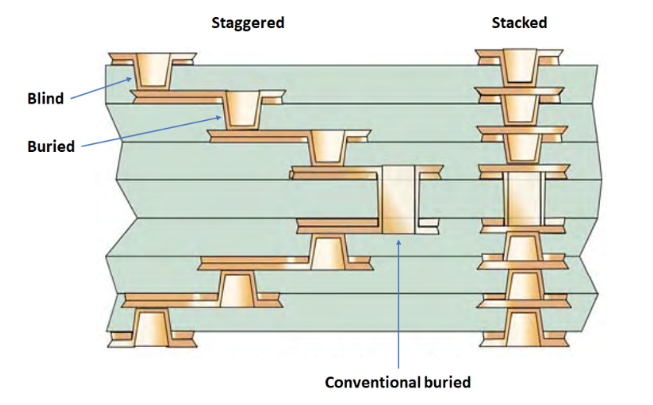
- Blind & Buried Vias, Stacked & Staggered Vias
- Conductive & Non-Conductive Via Plugging
- Min. 1.5/1.5 mil Line/Space
- Back Drill, Backplane, Embedded Devices, IC Substrate
Get a free quote now!
What is HDI PCB?

Get a free quote now!
HDI PCB stands for High-Density Interconnect Printed Circuit Board. This advanced PCB technology features smaller traces, smaller drill sizes, and more densely packed components. The thin traces connect the components, and the low current carrying capacity makes it suitable for high-density designs. Unlike traditional through-hole vias, HDI PCBs use micro vias, blind vias, and buried vias. These design innovations allow more components to be efficiently placed, optimizing space and routing. The technology is governed by industry standards such as IPC-2315, IPC-2226, IPC-4104, and IPC-6016.
Main Features of HDI PCB
HDI circuit boards often feature at least four layers, with most boards ranging from 6 to 12 layers due to their complexity and the need for numerous connections.
Small Trace Width and Spacing: Less than 4 mil
HDI PCBs require micro vias smaller than 6 mils, often stacked between layers and sometimes plated or filled. Via-in-pad (VIP) technology is used for increased density, optimizing the breakout area for routing.
HDI boards often undergo several rounds of stack-ups and lamination to integrate multiple blind and buried vias. These high-density layers are coupled with a thin dielectric and thick core layers.

Advantages of HDI Printed Circuit Boards
Smaller size and weight are achieved without sacrificing functionality.
Although HDI manufacturing can be costly, it reduces overall application costs by compacting components.
HDI PCBs offer improved signal integrity and reduced noise, with micro vias and blind vias enabling superior performance.
Production processes for HDI PCBs are efficient, leading to faster turnarounds.

Applications of HDI PCB
Automotive Systems:
HDI PCBs power vehicle control units and display drivers, essential for high-speed processing in modern vehicles.
Consumer Electronics:
Devices like smartphones, tablets, and smartwatches rely on HDI PCBs for high performance and high-definition displays.
Defense & Aerospace:
HDI PCBs are integral to high-powered defense and aerospace applications due to their precision, lightweight design, and high computational capacity.
Medical Devices:
Advanced medical tools and equipment, such as robotic arms and precise laser systems, use HDI technology for reliable, compact performance.
Challenges of HDI Circuit Boards
HDI PCBs present several design challenges:
- Small area with tightly packed components.
- Both sides of the PCB are often populated with components.
- Complex routing with numerous nets and traces.
Key Considerations for HDI PCB Design and Manufacturing
HDI design must account for multiple factors:
- Layer Count: Typically determined by BGA IC requirements and routing needs.
- Manufacturing Capabilities: Must align with the design, especially regarding via placement, stack-ups, and trace width.
- Reliability: Assembly and real-world usage must not compromise the board’s reliability.
Manufacturing Constraints in HDI PCBs
The manufacturing of HDI PCBs involves several challenges, including handling smaller components and ensuring the core materials meet electrical and mechanical performance standards. Design for Manufacturing (DFM) principles must guide the production process, especially in regard to substrate considerations like copper adhesion and dielectric stability.

ESPCBA: A China HDI PCB Manufacturer with 16+ Years of Experience
As a leading HDI PCB manufacturer in China, ESPCBA offers:
Highest Industrial Quality Standards:
Adhering to ISO9001, ISO13485, TS16949, and IPC-A-600 Class 2, 3, and 3A standards.
Advanced Equipment and Technology:
Our facility is equipped to handle complex PCB designs, including stacked and staggered blind vias and VIPPO technology.
No Minimum Order Quantity:
We welcome orders starting from just one piece.
One-Stop Services:
From material selection to shipping, our turnkey solutions simplify the process for you.
Excellent Pre-sales and After-sales Services:
Dedicated support ensures a seamless experience.
Connect with us
Get an Instant Online Quote Today
Looking for reliable SMD assembly services? At ESPCBA, we’re your trusted partner for PCB fabrication, component sourcing, and electronic manufacturing. With over 16 years of experience, we’ve provided high-quality PCBs at competitive prices to over 1,000 customers worldwide. Our company is ISO9001:2015 certified and UL listed, and every product we deliver is 100% E-tested and inspected using AOI and X-ray to meet the highest standards. Get an instant quote from our sales team today, and let us handle the rest for you.
Frequently Asked Questions
HDI PCBs are multi-layer boards with high circuit density and via sizes smaller than 0.15mm.
HDI PCBs offer smaller form factors, reduced weight, and enhanced electronic performance.
Higher costs due to small drill sizes and longer lead times for production.
Pricing depends on factors like layer count, via structure, and surface finishes. Contact our sales team for a customized quote.
Designers should consider tips like minimizing complexity, managing signal integrity, and optimizing material costs.
The manufacturing process involves several steps, including core board fabrication, CO2 laser drilling, hole metallization, and AOI inspection.