Modern consumer devices like smartphones, wearables, and smart home systems rely on advanced circuit boards that combine precision with affordability. As demand grows, manufacturers face intense pressure to deliver large-scale production runs without sacrificing reliability or profitability. This challenge requires a delicate balance between three critical factors: cost efficiency, rapid turnaround, and consistent quality.
Automation plays a vital role in achieving this balance. Advanced assembly lines can produce thousands of units daily while minimizing errors. For projects exceeding 10,000 units, economies of scale kick in dramatically. Bulk material procurement and optimized workflows reduce per-unit expenses, creating competitive pricing structures.
We’ve observed that successful operations prioritize scalable processes from the start. Rigorous testing protocols ensure each board meets performance standards, even at maximum output levels. This approach helps manufacturers adapt to shifting market demands while maintaining profit margins in fast-paced electronics sectors.
Key Takeaways
- Automation drives both speed and consistency in large-scale production
- Per-unit costs decrease significantly at volumes above 10,000 units
- Scalable processes prevent quality compromises during expansion
- Market competitiveness depends on adaptable manufacturing strategies
- Bulk material sourcing optimizes supply chain efficiency
Introduction to High-Volume PCBA for Consumer Electronics
From life-saving medical devices to cutting-edge automotive tech, advanced circuit boards are essential for seamless functionality. These intricate systems form the operational core of modern devices, requiring meticulous engineering to meet diverse industry demands.
Evolving Landscape of Device Manufacturing
We’ve witnessed how modern electronics manufacturing hinges on tightly integrated components. Compact designs now pack more processing power than entire rooms of equipment from a decade ago. This evolution demands precision-engineered boards that maintain signal integrity while resisting environmental stressors.
Our experience shows that successful projects begin with strategic material selection. Components must withstand thermal fluctuations and mechanical stress without inflating costs. This delicate equilibrium separates market leaders from competitors struggling with recalls or warranty claims.
Strategic Priorities in Device Creation
Three factors dominate every production decision in this space. First, component traceability ensures consistent performance across batches. Second, scalable processes allow rapid response to shifting demand. Third, rigorous testing protocols catch defects before products reach consumers.
We prioritize partnerships with suppliers who understand these dynamics. As one industry expert noted: “The difference between profit and loss often comes down to millimeter-level design optimizations.” This reality drives our focus on DFM principles from initial prototyping through final assembly.
Understanding the Challenges in High-Volume PCB Assembly
In mass production, minor inefficiencies multiply rapidly, threatening project viability. We’ve found that success hinges on addressing two core challenges: managing variable expenses and maintaining defect-free output across thousands of units.
Key Cost Drivers in Consumer Electronics
Component selection dramatically impacts budgets. High-demand parts often carry premium pricing, while scarce components create delays. Multi-layer designs add hidden expenses through extended machining time and specialized labor requirements.
Production scale reveals another critical factor. While large orders reduce per-unit tooling costs, they magnify material waste if designs aren’t optimized. Automated assembly lines lower labor expenses but require significant upfront investment in equipment calibration.
Quality Control and Reliability Issues
A 0.5% defect rate becomes catastrophic at 50,000 units. We implement statistical process controls to catch deviations early, using X-ray inspection and functional testing. As one partner noted: “Reliability isn’t an option—it’s the price of entry in modern electronics.”
Environmental stressors like thermal cycling expose weaknesses in solder joints and trace integrity. Our teams conduct accelerated life testing to simulate years of use within weeks, ensuring products withstand real-world conditions without premature failure.
Design for Manufacturability in PCB Assembly

Smart manufacturing begins at the drawing board, where design choices dictate production outcomes. We implement design-manufacturability principles to eliminate bottlenecks before prototyping starts. This proactive approach reduces rework and ensures designs align with production capabilities.
Optimizing PCB Layouts and Layer Configurations
Layer count directly impacts both complexity and budget. Our analysis shows 2-layer boards handle 73% of consumer device requirements while costing 40% less than 4-layer alternatives. Strategic component placement minimizes cross-layer jumps, reducing signal interference risks.
| Layer Count | Avg. Cost | Typical Use Cases | Design Complexity |
|---|---|---|---|
| 2-layer | $0.85/unit | Basic controllers | Low |
| 4-layer | $1.45/unit | IoT devices | Medium |
| 6-layer | $2.10/unit | High-speed computing | High |
Minimizing Via Usage for Cost Efficiency
Each via adds $0.002-0.005 to production costs. We maintain densities below 80 vias/sq in through three strategies:
- Component clustering reduces trace lengths
- Double-sided placement optimizes routing
- Via-in-pad techniques for high-density areas
Standardized footprints (0805/0603) prevent custom tooling fees. As noted in our cost-effective manufacturing strategies, tolerance relaxation (±10%) avoids 12-18% additional machining steps. This precision balancing act enables mass production without quality compromises.
Component Selection for Cost-Effective PCB Assembly
 showcasing an array of electronic components. The foreground features neatly arranged capacitors, resistors, and integrated circuits, their metallic leads and pins shimmering under crisp lighting. The middle ground displays the intricate copper traces and solder masks, hinting at the board's complex interconnections. In the background, a blurred silhouette of additional PCB layers suggests the depth and density of the overall assembly. The scene conveys a sense of precision, organization, and the meticulous attention to detail required in component selection for cost-effective PCB manufacturing.")
Effective component choices form the backbone of affordable electronics manufacturing. We’ve found that 62% of project budgets can be optimized through strategic part selection without compromising performance. The right balance between standardization and customization determines both profitability and reliability in mass production.
Standardized vs Specialized Components
Generic parts offer hidden advantages beyond immediate cost savings. Off-the-shelf regulators and connectors reduce design complexity while improving supply chain stability. As one procurement manager noted: “Standardization cuts sourcing time by 40% compared to custom solutions.”
Bulk purchasing amplifies these benefits. High-usage items like 0805 resistors or ceramic capacitors see 15-30% price reductions at 50,000-unit quantities. We maintain real-time market data to identify optimal buying windows, locking in pricing before seasonal shortages occur.
Lead time analysis prevents costly production delays. Components with 12+ week deliveries often require expensive air freight or last-minute redesigns. Our teams cross-reference multiple suppliers to build redundancy into every bill of materials.
| Component Type | Cost Savings | Lead Time Advantage |
|---|---|---|
| Generic ICs | 22-35% | 2-4 weeks |
| Custom ASICs | 0-8% | 12-16 weeks |
| Standard LEDs | 18-27% | 1-3 weeks |
This strategic approach extends beyond initial procurement. We develop component libraries that streamline future projects, reducing engineering hours by 25% per new product iteration. The result? Faster time-to-market with predictable manufacturing costs.
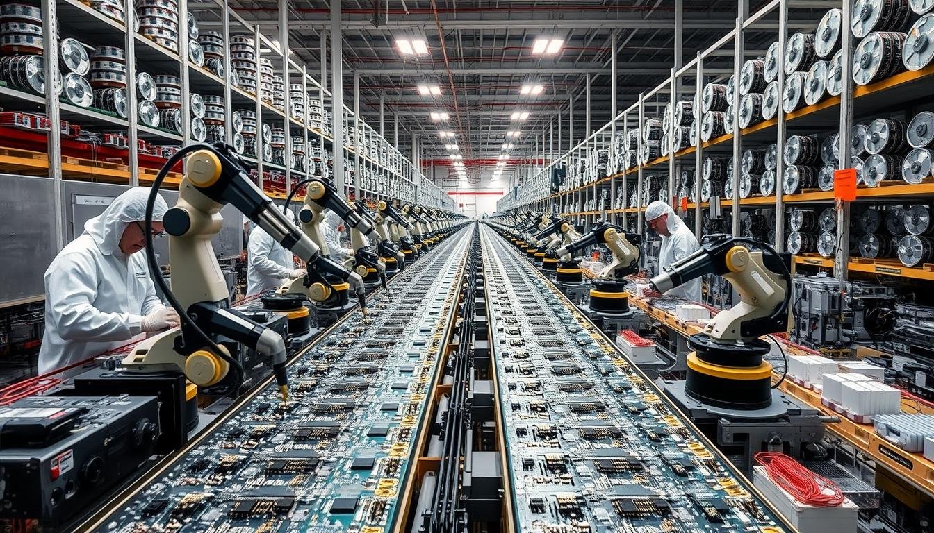
Harnessing Automation and Advanced Assembly Processes
Advanced manufacturing techniques redefine efficiency in electronics production. We implement robotic systems that handle complex tasks with micron-level precision, creating a foundation for scalable operations. Automated pick-and-place machines position components at speeds exceeding 25,000 placements per hour, slashing production timelines while maintaining accuracy.
Benefits of Automated Optical Inspection
Our quality assurance relies on automated optical inspection (AOI) systems. These vision-based scanners detect solder defects and misaligned parts faster than human inspectors. Real-time feedback loops correct assembly line parameters, preventing batch failures. AOI reduces rework costs by 38% in high-volume runs.
Surface Mount Technology Advantages
Surface mount technology (SMT) enables compact, high-density board designs. Automated solder paste application ensures consistent joint formation across thousands of connections. We achieve 99.98% placement accuracy through vision-guided robotics, critical for miniaturized consumer devices.
These processes work synergistically to eliminate bottlenecks. Thermal profiling optimizes solder reflow ovens, while inline testing validates each board’s functionality. The result? Scalable manufacturing that meets market demands without compromising reliability.