Electromagnetic interference (EMI) is a ubiquitous issue in modern electronics, affecting device performance and signal integrity. As electronic devices become increasingly dense and high-speed, noise issues can severely impact functionality. We explore comprehensive strategies for minimizing EMI and electromagnetic compatibility (EMC) issues through intelligent printed circuit board assembly (PCBA) layout techniques.
Proper PCB design is crucial in reducing EMI/EMC problems. By implementing strategic planning in the early design stages, engineers and designers can prevent costly redesigns and compliance failures, saving time and resources in the product development cycle.
Key Takeaways
- Understand the importance of PCB design in minimizing EMI/EMC issues.
- Learn how intelligent PCBA layout techniques can improve signal integrity.
- Discover strategies for reducing electromagnetic interference in high-speed electronic designs.
- Explore the benefits of early design stage planning in preventing costly redesigns.
- Gain insights into optimizing PCB design for better performance.
Understanding EMI/EMC Fundamentals in PCB Design
Electromagnetic interference (EMI) and electromagnetic compatibility (EMC) are crucial considerations in modern PCB design. As we delve into the world of PCB design, it’s essential to understand the basics of EMI and EMC to ensure the reliability and performance of electronic devices.
What Are EMI and EMC in PCBs?
EMI refers to the unwanted electromagnetic energy that disrupts the normal operation of electronic circuits. EMC, on the other hand, is the ability of electronic devices to function correctly in their electromagnetic environment without introducing intolerable electromagnetic disturbances to other equipment. In PCBs, EMI can manifest through conducted and radiated emissions, corrupting signal quality and causing malfunctioning.
Why EMI/EMC Matters in Modern Electronics
In modern electronics, higher frequencies, greater integration density, and stricter regulatory requirements make EMI/EMC considerations increasingly critical. Signal integrity problems caused by EMI can lead to intermittent failures, data corruption, and reduced performance. Ensuring EMC is not just about regulatory compliance; it’s also about guaranteeing product reliability and customer satisfaction.
The Cost of Ignoring EMI/EMC in Early Design Stages
Ignoring EMI/EMC in the early design stages can have significant financial implications, including costly redesigns, failed compliance testing, delayed market entry, and potential product recalls. A well-planned EMI/EMC strategy can mitigate these risks, ensuring a smoother path to market.
| EMI/EMC Consideration | Impact on PCB Design | Consequence of Ignoring |
|---|---|---|
| Conducted Emissions | Noise on power and signal lines | Failed compliance testing |
| Radiated Emissions | Electromagnetic radiation from PCB | Interference with other devices |
| Signal Integrity | Data corruption and reduced performance | Intermittent failures and customer dissatisfaction |
Common Sources of EMI in PCB Designs
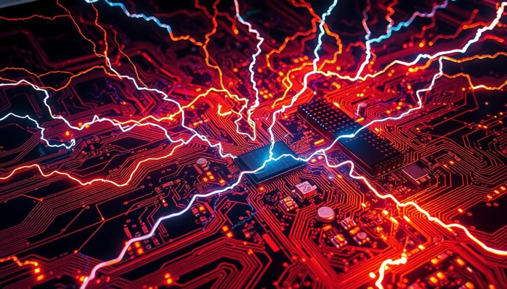
Identifying common sources of EMI in PCB designs is essential for developing effective strategies to minimize its impact on electronic systems. EMI can arise from various sources, including conducted and radiated emissions, common and differential mode currents, and high-frequency traces and switching devices.
Conducted vs. Radiated Emissions
EMI can be categorized into conducted and radiated emissions. Conducted emissions enter the system through power input lines and cables, while radiated emissions occur due to electromagnetic waves from power and communication lines, switching devices, and electrostatic discharges. Understanding the difference between these two types of emissions is crucial for implementing effective mitigation strategies.
| Emission Type | Description | Mitigation Strategies |
|---|---|---|
| Conducted Emissions | Enter through power lines and cables | Filtering, shielding |
| Radiated Emissions | Electromagnetic waves from devices and traces | Shielding, grounding, layout optimization |
Common Mode vs. Differential Mode Currents
Currents in PCB designs can be classified into common mode and differential mode currents. Common mode currents flow in the same direction in multiple conductors, while differential mode currents flow in opposite directions. Poor decoupling practices can result in unintentional common and differential mode currents, leading to EMI.
High-Frequency Traces and Switching Devices
High-frequency traces can act as unintentional antennas, converting electrical energy into electromagnetic radiation. Switching devices like transistors and MOSFETs can generate EMI due to fast rise and fall times, creating higher frequency harmonics. Proper design and layout techniques are essential to minimize the impact of these components on EMI.
By understanding these common sources of EMI, we can develop targeted strategies to reduce electromagnetic interference in PCB designs, ensuring the reliability and performance of electronic systems.
Ground Plane Optimization Techniques for EMI Reduction
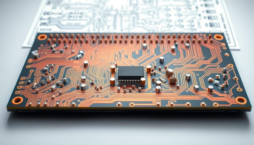
Ground plane optimization stands as a foundational element in the quest to reduce EMI in electronic circuits. A well-designed ground plane provides low-impedance return paths, which are essential for minimizing loop areas and reducing electromagnetic radiation.
Implementing Full Ground Planes vs. Ground Grids
When designing a PCB, choosing between a full ground plane and a ground grid is crucial. A full ground plane offers the least inductance value, reducing EM emission and crosstalk. However, in scenarios where a dedicated ground layer isn’t feasible, such as in a two-layer PCB, ground grids become a viable alternative.
Minimizing Return Path Loops
To minimize return path loops, it’s essential to ensure that high-speed signals have an uninterrupted ground plane directly beneath them. This reduces the effective loop area, consequently decreasing EMI. We achieve this by maintaining ground plane continuity, particularly for high-speed signals where impedance control is critical.
Using Faraday Cages and Guard Rings
Faraday cages and guard rings are effective techniques for isolating sensitive circuits or containing noisy components. By implementing these techniques, we can significantly reduce EMI. For instance, guard rings around high-frequency components can prevent noise from radiating outward.
Proper Grounding of Copper Fill Areas
Properly grounding copper fill areas is vital to prevent them from becoming unintentional antennas. Techniques such as stitching vias and strategic connection points ensure that these areas do not contribute to EMI. By grounding these areas effectively, we maintain signal integrity and reduce electromagnetic radiation.
In conclusion, optimizing the ground plane is a multifaceted approach that involves choosing the right ground plane configuration, minimizing return path loops, and using techniques like Faraday cages and guard rings. By implementing these strategies, we can significantly reduce EMI in PCB designs, ensuring better performance and compliance with EMC standards.
Smart Trace Routing to Minimize EMI/EMC Issues
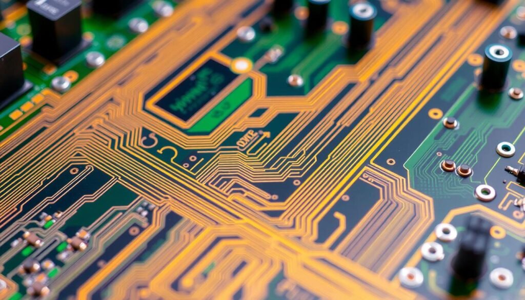
Effective trace routing is crucial for minimizing EMI/EMC issues in PCB design. Traces are the conductive paths that carry current from the driver to the receiver on the PCB. When these traces come across any bend or cross, they form a fully radiating antenna.
Trace Separation and the 3W Rule
The separation between traces should be at least three times the trace width (3W rule). This practice helps reduce crosstalk and coupling between adjacent traces on the same PCB layer, minimizing noise and ensuring signal integrity.
Routing Differential Pairs Effectively
Differential pairs require careful routing to maintain consistent spacing and length matching. Avoiding splits in reference planes is crucial to prevent compromising common-mode rejection, which can lead to EMI issues.
Via Placement Best Practices
Vias introduce impedance discontinuities and can create return path issues if not properly managed. Using ground vias nearby can mitigate these effects, ensuring a clean signal path.
Avoiding Stubs in High-Frequency Traces
Stubs in high-frequency traces can cause signal reflections and resonance effects, significantly increasing EMI. Techniques like using via-in-pad or optimizing trace lengths can help avoid these issues.
By implementing these smart trace routing techniques, you can dramatically reduce EMI/EMC issues in your PCB designs. Proper trace routing ensures the electromagnetic compatibility of your PCBs, leading to more reliable and efficient electronic systems.
Strategic Component Placement for EMI Control
Strategic placement of components on a PCB is a foundational element in controlling electromagnetic interference. By carefully planning the layout of components, designers can significantly reduce the risk of EMI issues that can compromise the performance of electronic devices.
Segregating Analog and Digital Sections
One of the fundamental practices in EMI control is segregating analog and digital sections on a PCB. This separation prevents digital switching noise from corrupting sensitive analog signals. By grouping components according to the signals they operate on, such as analog, digital, and power supply, designers can ensure that signal tracks for each component group remain within their defined areas, thus minimizing potential interference.
As Henry W. Ott, a renowned expert in EMI/EMC, once said, “The key to successful EMI control is to understand the return currents and to design the PCB accordingly.” This emphasizes the importance of a well-planned PCB layout in managing EMI.
Decoupling Capacitor Placement Techniques
Decoupling capacitors play a crucial role in reducing power rail noise caused by ICs switching current at high frequencies. To effectively filter this noise, decoupling capacitors should be placed as close as possible to the IC power pins. Proper grounding approaches and sizing strategies are also critical in ensuring that these capacitors can effectively filter power supply noise across different frequency ranges.
Positioning of High-Speed and Noise-Sensitive Components
The positioning of high-speed components, such as clock generators and microprocessors, away from noise-sensitive circuits is another critical aspect of EMI control. By carefully placing these components, designers can minimize the coupling between critical signal paths and potential noise sources. This strategic placement, combined with careful consideration of component orientation, can significantly reduce EMI in challenging designs.
By implementing these strategies, designers can create PCBs that are more resilient to EMI, ensuring the reliability and performance of electronic devices.
PCB Layer Stack-Up Optimization
We explore how PCB layer stack-up optimization can significantly reduce EMI/EMC issues. The layer stack-up is a fundamental design decision that impacts the EMI/EMC performance of a PCB by determining the reference planes available for signals and the coupling between power and ground planes.
Ideal Layer Arrangements for 2-Layer PCBs
For 2-layer PCBs, optimizing the layer stack-up is challenging due to the limited number of layers. One effective strategy is to use a ground grid to provide a return path for currents. Strategic trace routing is also crucial; for instance, using orthogonal routing on the two layers can help minimize crosstalk. While a dedicated ground plane is not feasible, careful design can still mitigate EMI issues.
Recommended Stack-Up for 4-Layer PCBs
The preferred stack-up for a 4-layer PCB is signal-ground-power-signal. This configuration provides a continuous ground plane, which is essential for controlling EMI. The ground plane acts as a shield for the signals on the adjacent layers. The power plane is placed adjacent to the ground plane to provide good decoupling and minimize impedance. Impedance-matched traces should be routed on the signal layers, preferably on the layer closest to the ground plane.
Multi-Layer PCB Stack-Up Strategies
For multi-layer PCBs, advanced stack-up strategies can balance signal integrity, power integrity, and EMI control. Using closely coupled power-ground plane pairs can enhance decoupling and reduce EMI. Multiple ground planes can be used to further improve EMI performance. It’s also beneficial to bury high-speed signals between ground planes to minimize radiated emissions. Collaboration with the PCB fabricator is crucial to ensure the stack-up design is manufacturable and meets the required performance specifications.
Shielding and Isolation Methods to Reduce EMI/EMC Issues Through Smart PCBA Layout
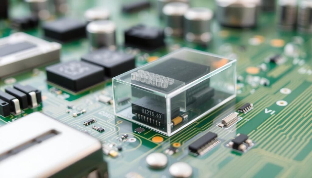
When optimizing PCB layout alone isn’t enough, shielding and isolation methods become essential. Shielding is a mechanical technique that uses conductive or magnetic materials to prevent EMI in the system. A mechanical shield is a closed conductive container connected to the ground, effectively reducing the size of loop antennas by absorbing and reflecting a part of their radiation.
Board-Level Shielding Options
We explore various shielding options at the board level, including SMT shield cans, conformal shielding, and embedded shielding layers. These solutions can be tailored to different applications, providing effective EMI protection.
Cable Shielding Considerations
Proper shielding of cables is crucial to prevent them from becoming sources or victims of EMI. Techniques for effective cable shielding include proper shield termination methods.
Implementing Controlled Impedance for Transmission Lines
Maintaining consistent impedance in transmission lines reduces reflections and standing waves, thereby minimizing emissions. This is crucial for ensuring signal integrity and reducing interference.
By implementing these shielding and isolation techniques, we can significantly reduce EMI/EMC issues in PCBA designs. For more detailed guidance on optimizing PCB designs for EMI/EMC, visit our resource page at ProtoExpress.
Conclusion: Implementing EMI/EMC-Friendly Design Practices
Effective EMI/EMC design is not just about compliance; it’s about creating products that perform consistently in real-world environments. By integrating the strategies outlined in this article, designers can significantly minimize EMI and enhance signal integrity.
We have discussed various EMI/EMC reduction techniques, including ground plane optimization, smart trace routing, strategic component placement, and PCB layer stack-up optimization. These practices work together to create electromagnetically compatible PCB designs. Addressing EMI/EMC concerns early in the design process is crucial, as proactive design is far more cost-effective than reactive fixes after problems are discovered during testing.
A practical implementation roadmap involves careful component selection, layout planning, detailed routing, and final verification. Simulation and pre-compliance testing are essential steps in verifying that your design meets EMI/EMC requirements before final production. These design techniques apply across various application domains, from consumer electronics to medical devices and industrial equipment.
As we move towards next-generation technologies like 5G and IoT devices, mastering PCB layout techniques for EMI/EMC control becomes increasingly important. By adopting these practices, designers can create robust, reliable products that deliver clean signals and minimal interference, ensuring optimal performance in demanding applications.
FAQ
What is the role of a ground plane in minimizing electromagnetic interference (EMI) in PCBA design?
How can trace routing impact EMI in PCB designs?
What are the benefits of using a full ground plane versus a ground grid in PCBA layout?
Why is component placement critical in controlling EMI?
What is the purpose of shielding in EMI/EMC control, and how can it be effectively implemented?
How does the layer stack-up in a PCB impact EMI/EMC performance?
What are some best practices for via placement in high-frequency PCB designs?
Can you explain the difference between conducted and radiated emissions in the context of EMI?
About The Author
Elena Tang
Hi, I’m Elena Tang, founder of ESPCBA. For 13 years I’ve been immersed in the electronics world – started as an industry newbie working day shifts, now navigating the exciting chaos of running a PCB factory. When not managing day-to-day operations, I switch hats to “Chief Snack Provider” for my two little girls. Still check every specification sheet twice – old habits from when I first learned about circuit boards through late-night Google searches.
