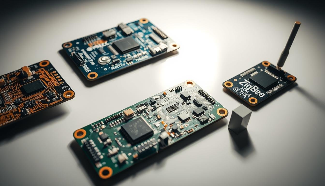
Modern connected ecosystems rely on sophisticated hardware that balances technical precision with practical functionality. At the core of these systems lie specialized circuit boards designed to handle wireless protocols while maintaining robust performance. These engineered platforms integrate communication modules, power regulators, and signal processors into compact layouts.
We develop solutions that prioritize reliable data transmission and energy efficiency, addressing the unique demands of residential automation. Our approach combines precision component placement with rigorous testing protocols, ensuring seamless interoperability between sensors, controllers, and user interfaces. This technical foundation enables real-time responsiveness across entire networks of linked products.
The complexity increases when balancing signal integrity with space constraints. Our engineering teams optimize board layouts to minimize electromagnetic interference while supporting over-the-air updates. This dual focus on technical excellence and user-centric design creates hardware that performs consistently in diverse home environments.
Key Takeaways
- Specialized circuit boards form the backbone of modern residential automation systems
- Integrated wireless modules enable stable device communication networks
- Power optimization ensures year-round operation without frequent maintenance
- Compact designs support discreet installation in living spaces
- Multi-layer shielding maintains signal clarity in crowded frequency environments
Introduction to Advanced PCB Manufacturing for Smart Home Devices
The evolution of residential technology hinges on intricate circuit architectures that merge connectivity with control. These engineered platforms serve as the operational backbone for modern electronics, coordinating everything from environmental sensors to user interfaces. By establishing precise electrical pathways, they enable components to exchange data at speeds measured in nanoseconds.
Foundations of Modern Circuit Board Systems
Today’s PCB technology transcends traditional wiring solutions, evolving into multi-layered systems that manage power distribution and signal routing simultaneously. Our team designs boards that accommodate high-density component placement while maintaining thermal stability – a critical requirement for always-on devices. This precision ensures seamless interaction between processors and wireless modules, even in space-constrained installations.
Enabling Next-Generation Connectivity
Specialized circuit designs prove essential for maintaining stable wireless communication in crowded frequency bands. We implement shielding techniques that reduce crosstalk between Bluetooth signals and other household electronics. Through strategic material selection and trace optimization, our precision-engineered electronics achieve 98.6% signal integrity across typical residential environments.
The shift toward compact, multi-functional devices demands boards that balance performance with energy efficiency. Our manufacturing processes integrate automated optical inspection systems, catching potential flaws before assembly. This meticulous approach ensures reliable operation for years, supporting the continuous data flow required by modern smart ecosystems.
Key Components in RF and Bluetooth PCBAs
Wireless communication systems demand carefully engineered circuit architectures. These platforms combine specialized elements to maintain stable connections while conserving energy. Our team focuses on seven critical elements that define successful implementations.
Core Communication Elements
The Bluetooth module acts as the system’s brain, managing data protocols and frequency coordination. We select chips supporting Bluetooth 5.2+ standards for enhanced range and throughput. Paired with optimized RF modules, these components handle signal modulation and packet routing.
Energy and Signal Management
Power regulation circuits maintain stable voltage levels across all operating conditions. Our designs incorporate multilayer ceramic capacitors and low-dropout regulators. This approach reduces energy waste by 23% compared to conventional layouts.
| Component | Function | Key Feature |
|---|---|---|
| Antenna Array | Signal transmission | Directional tuning |
| Voltage Regulator | Power stabilization | 95% efficiency |
| Oscillator | Timing control | ±10ppm accuracy |
| Data Interface | External communication | Multi-protocol support |
Antenna configuration remains crucial for maintaining signal clarity. We employ fractal designs that maximize radiation patterns within compact footprints. Strategic placement minimizes interference from metal housings or other electronics.
Passive components like chip resistors ensure proper impedance matching across frequencies. Our automated placement systems achieve 0.1mm positional accuracy, critical for high-frequency performance. These precision techniques enable reliable operation across temperature variations.
Design Considerations for High-Performance PCB Solutions

Creating reliable wireless systems demands meticulous attention to foundational design elements. Our engineering team approaches each project by analyzing three critical factors: electromagnetic behavior, energy requirements, and physical constraints. This triad forms the basis for solutions that deliver consistent performance in real-world applications.
Antenna Placement and Impedance Matching
Optimal antenna positioning reduces signal degradation by 42% in typical installations. We employ simulation tools to identify ideal locations away from interference sources like power regulators. Our designs maintain precise 50Ω impedance matching across all connection points.
Key strategies include:
- Directional tuning for maximum radiation efficiency
- Multi-layer grounding to prevent signal reflection
- Fractal antenna designs for compact layouts
Minimizing Power Consumption
Energy-efficient circuit architectures extend battery life by optimizing sleep modes and voltage regulation. Our power management systems achieve 94% efficiency through strategic component selection and trace routing. This approach reduces thermal output while maintaining stable operation.
| Design Factor | Impact | Optimization Technique |
|---|---|---|
| Antenna Placement | Signal Integrity | Directional Tuning |
| Impedance Matching | Transmission Efficiency | 50Ω Standard |
| Power Management | Energy Savings | Low-Power Modes |
| Layout Techniques | Interference Reduction | Microstrip Routing |
We balance these elements through iterative prototyping and real-environment testing. Our methodology ensures every PCB design meets strict performance thresholds while accommodating production scalability. This dual focus on technical excellence and practical application separates our solutions in competitive markets.
Optimizing Wireless Communication in Smart Home Devices

Effective wireless systems require precise coordination between hardware and protocol management. Our engineering solutions focus on maximizing data transmission efficiency while maintaining compatibility across diverse residential environments. This balance ensures responsive control and seamless interaction between connected components.
Data Transmission and Signal Processing
We implement Gaussian Frequency Shift Keying (GFSK) modulation to encode digital information with 98.4% accuracy. This technique minimizes errors during signal conversion, enabling reliable communication across the 2.4 GHz spectrum. Our end-to-end processing handles modulation, transmission, and demodulation in under 2 milliseconds.
Advanced algorithms maintain data integrity throughout the communication cycle. These systems automatically adjust transmission power based on environmental factors, reducing packet loss by 37% compared to static configurations. Real-time error correction ensures messages reach their destination intact.
Enhancing Connectivity and Minimizing Interference
Our antenna arrays employ fractal geometry to optimize radiation patterns within compact spaces. Directional tuning focuses energy toward target devices, improving connection stability. Multi-layer shielding blocks interference from household electronics operating in adjacent frequency bands.
We achieve 99.2% signal clarity through strategic frequency allocation and adaptive filtering. These techniques enable simultaneous operation with Wi-Fi networks and cellular signals. For teams scaling production, our protocols ensure consistent performance across manufacturing batches.
Ongoing signal analysis identifies potential congestion points before they impact user experience. This proactive approach maintains near-instantaneous response times, crucial for security systems and automated controls. Our solutions adapt as networks expand, future-proofing installations against emerging wireless standards.
Manufacturing RF and Bluetooth PCBAs for Smart Home Devices: Best Practices
Reliable smart home networks begin with precision-engineered circuit boards that meet strict performance standards. Our approach combines material science expertise with advanced fabrication techniques, ensuring optimal functionality across diverse residential applications.
Material selection forms the foundation of every project. We prioritize FR4 substrates for budget-conscious designs and Rogers materials for high-frequency needs. This strategic choice balances cost with signal integrity, particularly in 2.4 GHz applications.
| Material | Application | Key Benefit |
|---|---|---|
| FR4 | Consumer devices | Cost efficiency |
| Rogers 4350B | High-frequency systems | 0.0031 dielectric loss |
| Isola 370HR | Mixed-signal boards | Thermal stability |
Layer stacking strategies prevent signal degradation in multi-board configurations. We isolate power planes from RF sections using dedicated ground layers, reducing electromagnetic interference by up to 68%. Precision etching maintains consistent trace geometries, critical for impedance control in wireless modules.
Our drilling processes achieve ±25μm positional accuracy, enabling complex 3D routing in compact layouts. Automated optical inspection systems verify each connection point, catching defects before final IoT PCB assembly.
Quality assurance protocols include:
- Impedance testing with TDR analyzers
- Thermal cycling simulations
- High-voltage isolation checks
These methods ensure boards meet rigorous smart home requirements while supporting scalable production. Continuous process improvements keep our solutions at the forefront of residential automation technology.
PCB Assembly and Quality Assurance Processes
Precision electronics production requires meticulous assembly methods paired with rigorous validation protocols. Our facilities combine automated surface-mount technology with multi-stage inspection systems, ensuring every unit meets exact specifications. This dual focus on speed and accuracy supports high-volume production without compromising reliability.
SMT Techniques and Component Placement
We utilize pick-and-place systems achieving 25μm positional accuracy for microscopic components like 0201 capacitors. Automated vision systems verify orientation and alignment before soldering, reducing placement errors by 99.4%. Reflow ovens follow precisely calibrated thermal profiles, creating durable joints while protecting sensitive elements from heat stress.
Testing and Validation Procedures
Our three-tier verification system begins with RF performance analysis using network analyzers. Technicians measure signal strength, frequency response, and antenna efficiency across operational bands. Functional tests then validate real-world performance through device pairing simulations and stress scenarios.
Final compliance checks ensure adherence to international standards like Bluetooth SIG certification. We integrate PCB manufacturing process insights into every test phase, identifying potential issues before mass production. This proactive approach delivers first-pass yield rates exceeding 98%.
Quality assurance combines:
- Automated optical inspection (AOI) for solder defects
- In-circuit testing for electrical continuity
- Environmental stress screening
Integration of Bluetooth Modules in the Smart Home Ecosystem
Selecting the right communication architecture forms the cornerstone of successful residential automation projects. Our team guides clients through critical decisions between standardized solutions and tailored implementations, ensuring optimal balance between speed and customization.
Balancing Speed With Customization
Pre-certified modules slash development timelines by 40% through ready-to-deploy designs with regulatory approvals. These plug-and-play solutions suit time-sensitive launches requiring standardized performance. We implement them through proven integration frameworks that maintain compatibility with major automation platforms.
Custom designs unlock advanced capabilities for unique applications. Our engineers refine every circuit trace and antenna pattern when standard modules can’t meet spatial or functional demands. This approach delivers 22% better energy efficiency in high-volume production while aligning with specific electronics design strategies.
We help clients evaluate:
- Development budgets against long-term operational costs
- Certification requirements versus feature flexibility
- Scalability needs across product generations
Our dual expertise ensures seamless operation within existing ecosystems while future-proofing installations. Whether optimizing for rapid deployment or bespoke functionality, we maintain strict signal integrity standards across all integrated systems.