The miniaturization trend in modern electronics has driven the development of advanced packaging technologies like Micro-BGA (Ball Grid Array) and PoP (Package-on-Package). These technologies enable the high-density integration essential for smartphones, wearables, and IoT devices. However, their assembly presents significant technical challenges that require specialized knowledge and equipment. This article explores these challenges and provides practical solutions for electronics engineers and PCB designers seeking to optimize their assembly processes.
Understanding Micro-BGA and PoP Technologies
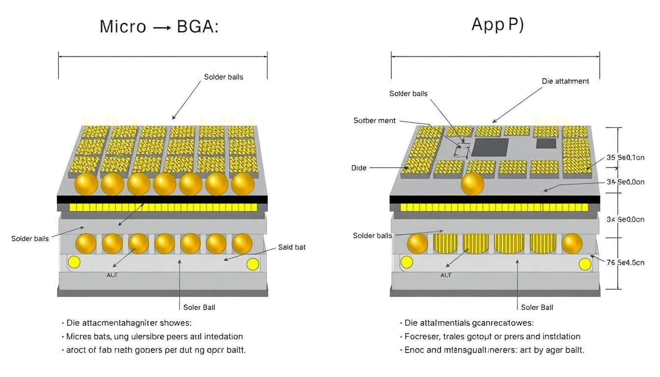
Figure 1: Cross-sectional view of Micro-BGA (left) and PoP (right) structures
Micro-BGA Technology
Micro-BGA (μBGA) is a miniaturized version of traditional BGA packaging, featuring significantly smaller solder balls and reduced pitch (typically under 0.5mm). Unlike conventional BGAs, Micro-BGAs are constructed on packaging tape with the die facing downward. An elastomer layer between the tape and die helps mitigate thermal expansion stress, making this technology ideal for compact, high-memory applications.
Package-on-Package (PoP) Technology
PoP assembly involves vertically stacking two or more semiconductor packages, typically combining a logic chip (processor or SoC) with memory components. This three-dimensional integration significantly reduces the PCB footprint while improving signal integrity by minimizing the distance between interconnected components. The stacked configuration enables faster data transmission and enhanced overall performance in space-constrained applications.
Applications in Modern Electronics
Both Micro-BGA and PoP technologies have become essential in various electronic devices where space efficiency and performance are critical:
- Smartphones and tablets
- Wearable technology
- IoT devices and sensors
- Portable medical devices
- Automotive electronics
- High-performance computing
- Networking equipment
- Advanced camera modules
Key Technical Challenges in Micro-BGA and PoP Assembly

Figure 2: Warpage visualization in a Micro-BGA package during reflow soldering
Miniaturization and High-Density Interconnects
The extremely fine pitch of Micro-BGA packages (often below 0.4mm) creates significant challenges for both design and manufacturing. The reduced spacing between solder balls increases the risk of bridging and requires exceptional precision during placement. For PoP assemblies, the complexity increases further as multiple packages must align perfectly to ensure reliable connections between stacked components.
Thermal Management During Reflow Soldering
The reflow soldering process for Micro-BGA and PoP assemblies requires precise temperature control. The challenge is particularly acute with PoP, where both packages must be reflowed simultaneously. Uneven heating can lead to incomplete solder joints in some areas while potentially damaging heat-sensitive components in others. The thermal profile must account for different thermal masses and expansion rates of the stacked packages.

Figure 3: Optimal reflow temperature profile for Micro-BGA and PoP assembly
Warpage and Misalignment Risks
Package warpage is a significant concern during the reflow process. As temperature increases, different materials expand at varying rates, causing the package to bend or warp. This warpage can lead to open connections (head-in-pillow defects) or misalignment between stacked packages in PoP assemblies. The risk increases with larger package sizes and thinner substrates commonly used in modern designs.
Solder Joint Reliability Under Mechanical Stress
The miniature solder joints in Micro-BGA and PoP assemblies are particularly vulnerable to mechanical stresses from thermal cycling, vibration, and physical impact. This vulnerability is amplified in portable devices that experience frequent handling and temperature variations. Ensuring long-term reliability requires addressing these stress factors during both design and assembly phases.
Facing Micro-BGA or PoP Assembly Challenges?
Our engineering team can analyze your specific assembly requirements and provide customized recommendations to improve yield and reliability.
Actionable Solutions for Micro-BGA and PoP Assembly
Advanced Reflow Ovens with Precise Temperature Profiling
Modern reflow ovens with multiple heating zones and advanced temperature control capabilities are essential for successful Micro-BGA and PoP assembly. These systems allow for customized thermal profiles that can be optimized for specific package combinations. Key features to look for include:

Figure 4: Multi-zone reflow oven with advanced temperature control capabilities
- Nitrogen atmosphere capability to reduce oxidation
- Uniform heat distribution across the entire PCB
- Real-time temperature monitoring with feedback control
- Programmable profiles with high precision (±1°C tolerance)
- Controlled cooling rates to minimize thermal stress
Use of Underfill Materials for Stress Mitigation
Underfill materials play a crucial role in enhancing the mechanical reliability of Micro-BGA and PoP assemblies. These epoxy-based compounds fill the space between the package and the PCB, distributing mechanical stresses and protecting the solder joints from failure due to thermal cycling or physical shock.

Figure 5: Underfill application for a Micro-BGA package showing capillary flow
| Underfill Type | Flow Characteristics | Thermal Performance | Reworkability | Best Applications |
| Capillary Flow | Excellent self-leveling | Good thermal cycling resistance | Limited | Consumer electronics |
| No-Flow | Applied before component placement | Moderate | Poor | High-volume production |
| Reworkable | Controlled flow | Good | Excellent | Prototype and high-value boards |
| Thermal Conductive | Thicker consistency | Excellent heat dissipation | Limited | High-power applications |
Automated Optical Inspection (AOI) Systems for Alignment
Advanced inspection systems are critical for ensuring proper alignment and solder joint quality in Micro-BGA and PoP assemblies. While traditional optical inspection has limitations for hidden solder joints, modern systems combine multiple technologies:

Figure 6: X-ray inspection image of a PoP assembly showing interconnections between stacked packages
Pre-Reflow Inspection
- Component placement verification
- Solder paste volume measurement
- Alignment accuracy confirmation
- Foreign material detection
Post-Reflow Inspection
- X-ray inspection for hidden joints
- Void detection in solder connections
- Head-in-pillow defect identification
- 3D measurement of solder joint profiles
Design-for-Manufacturing (DFM) Optimizations
Implementing DFM principles early in the design process significantly improves the manufacturability of Micro-BGA and PoP assemblies. Key optimizations include:

Figure 7: Optimized PCB layout for Micro-BGA showing pad design and escape routing
- Optimized pad design with proper solder mask openings
- Strategic via placement for thermal management
- Balanced copper distribution to minimize warpage
- Fiducial markers for precise component placement
- Consideration of thermal expansion coefficients in material selection
Real-World Examples and Case Studies
Smartphone PCB Assembly Line: Overcoming Warpage Issues

Figure 8: Smartphone PCB assembly line with specialized fixtures for Micro-BGA and PoP components
A leading smartphone manufacturer faced significant yield issues with their flagship device due to warpage-related connection failures in PoP assemblies. The problem was particularly acute during summer months when ambient temperatures in the factory were higher. After comprehensive analysis, the following solutions were implemented:
Implemented Solutions
- Modified reflow profile with extended pre-heating phase
- Installed precision cooling systems in the assembly area
- Implemented vacuum fixtures during reflow to minimize warpage
- Added real-time warpage monitoring with laser measurement
Results
- Reduced defect rate from 3.2% to 0.4%
- Eliminated seasonal variations in yield
- Improved overall reliability in field testing
- Decreased rework costs by 78%
Comparison of Underfill Material Performance in Automotive Applications

Figure 9: Thermal cycling test results comparing underfill material performance in automotive applications
An automotive electronics supplier conducted extensive testing to identify the optimal underfill material for Micro-BGA components in engine control units exposed to extreme temperature variations. Four different underfill materials were evaluated under accelerated thermal cycling conditions (-40°C to +125°C).
| Underfill Material | Glass Transition Temp | CTE (ppm/°C) | Cycles to First Failure | Relative Cost |
| Standard Epoxy | 130°C | 35 | 850 | 1.0x |
| Silica-Filled Epoxy | 145°C | 28 | 1250 | 1.4x |
| Ceramic-Filled Compound | 155°C | 22 | 1680 | 1.8x |
| Advanced Nano-Composite | 165°C | 18 | 2240 | 2.3x |
The study concluded that while the nano-composite underfill provided the best performance, the ceramic-filled compound offered the optimal balance between reliability and cost for most automotive applications. This case study demonstrates the importance of application-specific material selection in Micro-BGA and PoP assemblies.
Technical Diagrams and Visual References
Cross-Sectional View of PoP Stacking

Figure 10: Detailed cross-sectional view of a PoP assembly showing all layers and interconnections
Reflow Temperature Curve for Micro-BGA Assembly

Figure 11: Detailed reflow temperature profile with critical thresholds for Micro-BGA assembly
Emerging Trends and Future Developments

Figure 12: Advanced 3D IC integration technology showing the future evolution of package stacking
The field of advanced packaging continues to evolve rapidly, with several emerging technologies poised to address current limitations in Micro-BGA and PoP assembly:
3D IC Integration
The next evolution beyond PoP is true 3D IC integration, where multiple die are stacked and connected using through-silicon vias (TSVs). This approach eliminates the need for separate packages and further reduces signal path lengths, improving performance while reducing form factor. Current challenges include heat dissipation and testing complexity, but significant progress is being made in both areas.
Laser-Assisted Soldering
Laser-assisted soldering technologies offer precise, localized heating that can significantly reduce thermal stress during assembly. This approach is particularly valuable for temperature-sensitive components and can enable selective reflow of individual packages in a PoP stack. The technology allows for much finer control over the reflow process, potentially eliminating many current warpage-related issues.
Advanced Underfill Technologies
New underfill materials with self-healing properties and improved thermal conductivity are being developed specifically for Micro-BGA and PoP applications. These materials can repair minor cracks in solder joints while simultaneously improving heat dissipation, addressing two major reliability concerns simultaneously.
AI-Powered Process Optimization
Artificial intelligence and machine learning algorithms are increasingly being applied to optimize assembly processes. These systems can analyze vast amounts of process data to identify subtle correlations between manufacturing parameters and quality outcomes, enabling continuous process improvement beyond what human analysis could achieve.
Conclusion
Micro-BGA and PoP assembly technologies have become essential enablers for modern electronics miniaturization, but they present significant technical challenges that require specialized knowledge and equipment to overcome. By implementing the solutions discussed in this article—including advanced reflow profiling, appropriate underfill materials, comprehensive inspection systems, and DFM optimizations—manufacturers can significantly improve yield and reliability in these complex assemblies.
As the industry continues to push the boundaries of miniaturization and performance, staying current with emerging technologies and best practices will be essential for electronics engineers and PCB designers working with these advanced packaging methods. The future of electronics assembly lies in increasingly integrated and sophisticated approaches that build upon the foundation established by Micro-BGA and PoP technologies.
Need Expert Guidance for Your Micro-BGA or PoP Assembly Project?
Our team of specialists can help optimize your assembly process, improve yield, and enhance reliability. Contact us today for a personalized consultation or download our comprehensive technical guide.
Frequently Asked Questions
What is the minimum pitch size currently achievable for Micro-BGA assembly?
Current production capabilities allow for Micro-BGA pitches as small as 0.3mm, with research facilities demonstrating feasibility down to 0.25mm. However, pitches below 0.4mm typically require specialized equipment and processes, including laser-defined stencils and advanced optical inspection systems.
How does PoP assembly affect signal integrity compared to traditional side-by-side placement?
PoP assembly significantly improves signal integrity by reducing the physical distance between interconnected components, particularly between processors and memory. This shorter path length minimizes signal degradation, reduces electromagnetic interference, and allows for higher operating frequencies. Studies have shown up to 30% improvement in signal quality and reduced power consumption compared to traditional side-by-side placement.
What are the key considerations when selecting underfill materials for automotive Micro-BGA applications?
For automotive applications, underfill materials must withstand extreme temperature cycling (-40°C to +125°C), have low moisture absorption, and maintain reliability over a 10-15 year lifespan. Key parameters to evaluate include coefficient of thermal expansion (CTE), glass transition temperature (Tg), adhesion strength, and flow characteristics. Ceramic-filled compounds typically offer the best balance of performance and cost for most automotive applications.
Advanced X-ray inspection systems use angled views (oblique angle radiography) and tomographic techniques to create detailed images of hidden solder joints in PoP assemblies. These systems can detect voids, insufficient solder, bridging, and head-in-pillow defects between stacked packages. Modern systems incorporate AI-based defect recognition to automatically identify potential issues that might be missed by human inspectors.