Have you ever encountered a situation where a PCB assembly failed in the field, leaving you puzzled about the cause and the solution?
When a pcb fails, it can be due to various factors, including environmental conditions, component malfunctions, or manufacturing defects. Troubleshooting such failures requires a systematic approach to identify and resolve the underlying issues.
Understanding the common causes of failures and effective troubleshooting methodologies is crucial for engineers and technicians to diagnose and repair failed circuit boards. By following a structured approach, you can efficiently identify failure points and restore your pcb to proper functioning, ensuring the reliability of your electronic devices.
Key Takeaways
- Understand the common causes of PCB failures in the field.
- Learn a systematic approach to troubleshooting PCB failures.
- Identify the essential tools and inspection techniques for diagnosing issues.
- Implement effective repair solutions to restore PCB functionality.
- Enhance the reliability of your electronic devices through proper troubleshooting.
Understanding PCBA Field Failures
Understanding the causes and impacts of PCBA field failures is essential for maintaining product reliability. We recognize that no PCBA is invincible, and any design can eventually be stressed until catastrophic failure occurs. A successful design from a reliability perspective is one where the applied stresses are so extreme that they are highly unlikely to be encountered during operation in the product’s intended environment.
What Constitutes a Field Failure
A field failure refers to the malfunction of a PCBA during its operational life, outside of the controlled environment of the manufacturing or testing phase. Such failures can occur due to various factors, including environmental stressors, component malfunctions, manufacturing defects, or design issues. The quality and reliability of the PCB assembly (PCBA) play a crucial role in determining its susceptibility to field failures.
The Impact of PCBA Failures on Operations
PCBA failures in the field can have far-reaching consequences, including production downtime, customer dissatisfaction, and potential safety risks. Some of the key impacts include:
- For industrial applications, a single PCBA failure can halt entire production lines, resulting in significant financial losses.
- In medical devices, transportation systems, or defense applications, PCBA failures can have life-critical implications.
- Field failures often incur substantial costs related to warranty claims, field service visits, replacement parts, and potential product recalls.
- The reputational damage from recurring field failures can significantly impact a company’s market position and customer trust.
By understanding the full operational impact of failures, organizations can properly allocate resources to quality control, testing, and design improvements. Implementing proper failure tracking and analysis systems allows companies to identify patterns and address systemic issues before they affect larger portions of deployed products.
Common Causes of PCBA Field Failures
Understanding the common causes of PCBA field failures is essential for developing robust troubleshooting strategies. When a PCBA fails in the field, it can be due to a variety of factors, ranging from environmental conditions to inherent design or manufacturing issues.
Environmental Factors
Environmental factors play a significant role in PCBA field failures. Exposure to extreme temperatures, humidity, and vibration can cause components to degrade or fail. For instance, high humidity can lead to corrosion on the PCB, while extreme temperatures can cause solder joints to crack. Ensuring that the PCBA is designed and manufactured to withstand the intended operating environment is crucial.
Component Malfunctions
Component malfunctions are another common cause of PCBA field failures. This can be due to defective components, improper component selection, or component degradation over time. For example, a capacitor might fail due to excessive voltage or current, leading to a cascade of failures in the circuit. Selecting components that meet the required specifications and ensuring their quality is vital.
Manufacturing Defects
Manufacturing defects can also lead to PCBA field failures. Issues such as solder bridging, insufficient solder, or improper PCB assembly can result in faulty PCBAs. Implementing rigorous quality control measures during the manufacturing process can help mitigate these issues.
Design Issues
Design issues are a significant cause of PCBA failures. Problems such as inadequate thermal management, signal integrity issues, and improper component placement can lead to failures. For instance, inadequate thermal management in the PCB design can cause component overheating, while signal integrity problems can result in intermittent failures. Ensuring that the PCB design is robust and accounts for the operational requirements is essential.
- Inadequate thermal management can lead to component overheating and accelerated aging.
- Signal integrity problems, such as impedance mismatches or crosstalk, can cause intermittent failures.
- Improper component placement can result in solder joint failures or component damage.
- Design choices not accounting for the operating environment can lead to field failures.
By understanding these common causes of PCBA field failures, we can develop effective strategies for troubleshooting and prevention, ultimately enhancing the reliability of PCBAs in the field.
Essential Tools for PCBA Troubleshooting
Effective PCBA troubleshooting relies on a combination of basic testing equipment and advanced diagnostic tools. We utilize these tools to identify and resolve issues efficiently, ensuring the reliability of the PCB.
Basic Testing Equipment
For initial troubleshooting, basic testing equipment is essential. This includes a multimeter for measuring voltage, current, and resistance, as well as a power supply to test the PCBA under various conditions. An LCR meter is also valuable for verifying the characteristics of inductors, capacitors, and resistors. These tools enable us to perform a thorough test of the PCBA’s components and circuits.
Advanced Diagnostic Tools
For more complex issues, advanced diagnostic tools are necessary. An oscilloscope is particularly valuable for analyzing signal integrity issues in failed PCBAs. Modern digital oscilloscopes can capture, display, and analyze complex waveforms, helping to identify timing issues, noise problems, and signal degradation. Other advanced tools include thermal imaging cameras for identifying hotspots, logic analyzers for troubleshooting complex digital circuits, and X-ray inspection systems for examining hidden solder joints and internal PCB structures. These tools facilitate detailed analysis and test of the PCBA, enabling precise diagnosis and repair.
- Advanced diagnostic tools significantly enhance troubleshooting capabilities, with oscilloscopes being particularly valuable for analyzing signal integrity issues in failed PCBAs.
- Thermal imaging cameras can quickly identify hotspots on a PCBA that may indicate component failures or poor thermal design.
- Logic analyzers are essential for troubleshooting complex digital circuits, capturing multiple signal channels simultaneously.
Visual Inspection Techniques

Understanding the failure of a PCBA begins with a detailed visual inspection process. This initial step is crucial in identifying potential causes of failure, which can range from environmental factors to manufacturing defects.
Surface-Level Examination
A surface-level examination is the first step in visually inspecting a PCBA. This involves looking for obvious signs of damage or wear, such as cracks, corrosion, or burn marks on the PCB. We inspect the board’s surface to identify any irregularities that could indicate a failure.
Microscopic Inspection
For a more detailed analysis, microscopic inspection is employed. This technique allows us to examine the solder joints and other components closely, revealing issues such as micro-cracks or improper soldering that are not visible to the naked eye.
X-ray and Thermal Imaging
Advanced techniques include X-ray and thermal imaging. X-ray inspection is particularly useful for examining hidden solder joints, such as those in BGA connections. Thermal imaging, on the other hand, helps identify hotspots on the PCBA that may indicate component failures or poor thermal design, relating to excessive heat. As we analyze the PCB using these methods, we can gain a comprehensive understanding of the failure mechanisms.
Systematic PCBA Troubleshooting Process
The key to successful PCBA troubleshooting lies in a systematic and thorough examination of the circuit board and its components. When a PCBA fails in the field, it’s crucial to follow a structured process to identify the root cause of the failure.
Mapping the Circuit Board
To begin troubleshooting, we first need to understand the layout of the PCB. Mapping the circuit board involves identifying critical components and their connections. This step is essential for focusing our troubleshooting efforts on the most likely areas of failure.
Testing Power Supply and Voltage
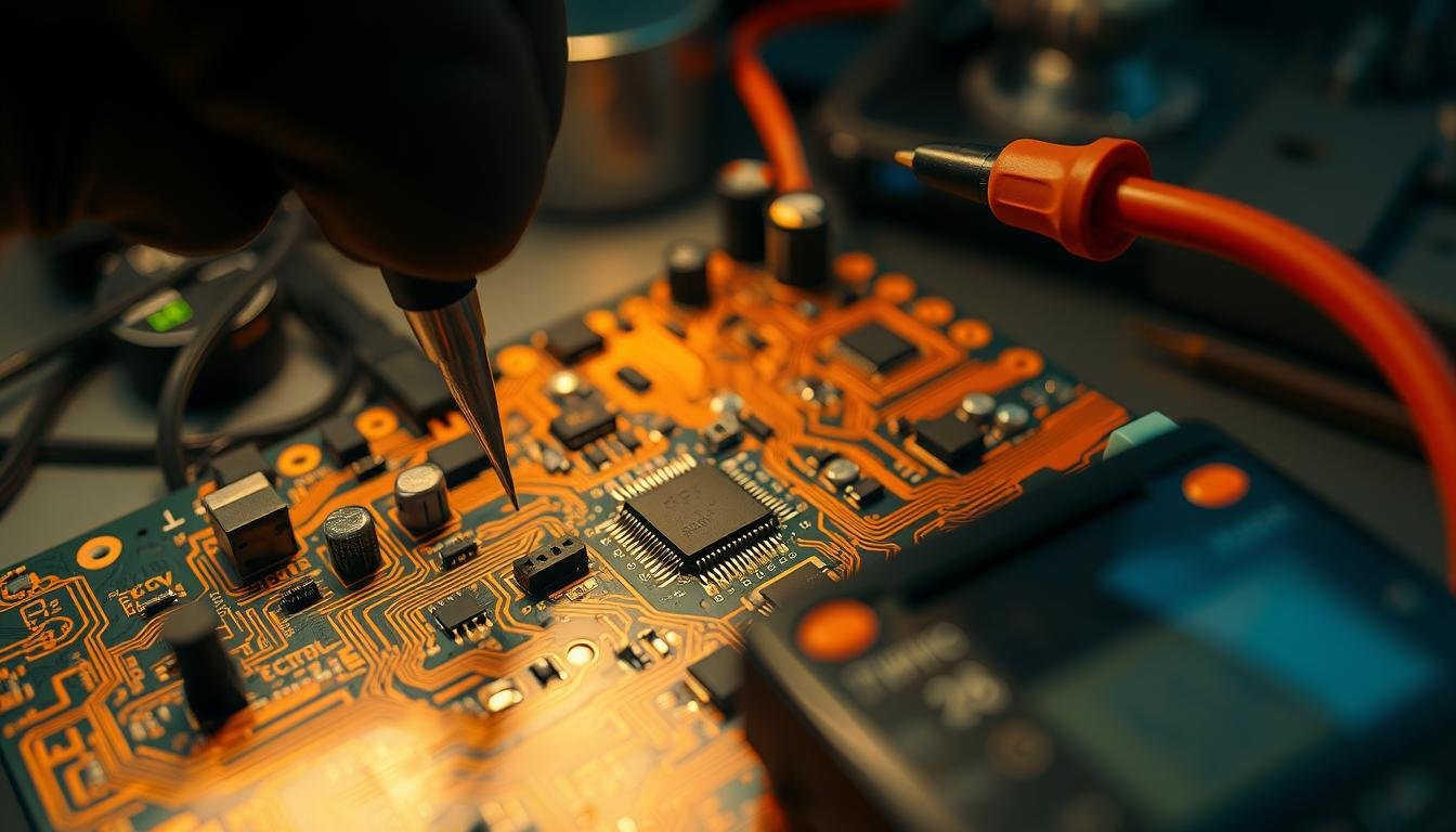
A crucial step in PCBA troubleshooting is verifying that the power supply is functioning correctly. We use tools like a multi-meter to check voltage levels across the PCB, ensuring they are within the specified ranges. This step helps identify any issues related to power distribution on the board.
Signal Testing and Analysis
Analyzing signals on the PCBA is vital for identifying any anomalies or issues. We employ various testing techniques to examine signal integrity, using equipment such as oscilloscopes and logic analyzers. This analysis helps pinpoint problems related to signal transmission or processing on the circuit.
Component-Level Testing
When broader functional tests indicate a failure in a specific section of the PCBA, we proceed to testing individual components. This involves using tools like multi-meters and LCR meters to test resistors, capacitors, inductors, diodes, transistors, and LEDs according to their datasheet specifications. For complex components or when in doubt, specialized component testers can provide more accurate results.
By following this systematic PCBA troubleshooting process, we can efficiently identify and address the root cause of failures, ensuring reliable operation of the PCB in the field.
My PCBA Failed in the Field: Repair Techniques

When a PCBA fails in the field, effective repair techniques are crucial to minimize downtime and restore functionality. We will explore various methods to address common issues, ensuring that the PCBA is restored to its optimal functioning state.
Repairing Broken Traces
Broken traces on a PCB can be a significant issue. To repair them, we first identify the break using a multimeter or visual inspection. Once located, we can use a conductive pen or wire to bridge the gap. For more severe damage, replacing the entire trace may be necessary. This involves carefully removing the damaged trace and soldering a new one in its place, ensuring that the connection is secure and reliable.
Replacing Defective Components
Defective components can cause a range of issues, from minor malfunctions to complete system failures. To replace them, we first desolder the faulty component, taking care not to damage surrounding components or the PCB. We then clean the area thoroughly before soldering the new component into place. It’s essential to use the correct soldering techniques and temperature profiles to ensure a reliable connection.
Addressing Solder Joint Issues
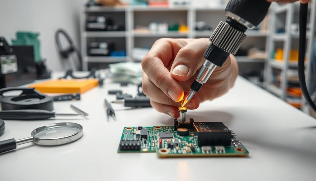
Solder joint issues are a common cause of PCBA failures, often resulting from thermal cycling or mechanical vibration. To address these issues, we reflow the solder joint using a soldering iron at 300-350°C, applying flux and adding a small amount of fresh solder to create a shiny, concave joint. Other indicators of solder joint issues include cold joints, excessive solder, and tombstoning. By reworking these joints and ensuring they meet IPC standards, we can significantly improve the reliability of the PCBA.
- Solder joint issues represent one of the most common causes of PCBA field failures, particularly in environments with thermal cycling or mechanical vibration.
- Reworking problematic solder joints requires proper flux application, appropriate temperature control, and the right amount of fresh solder.
- Inspecting reworked solder joints under magnification ensures they meet IPC standards for proper wetting, fillet formation, and surface appearance.
By employing these repair techniques, we can effectively address common PCBA issues, minimize downtime, and ensure the reliability of our electronics manufacturing solutions.
Preventing Future PCBA Failures
Preventing future PCBA failures requires a comprehensive strategy that addresses various factors, including design reliability and proper handling procedures. By understanding the causes of field failures and implementing preventive measures, we can significantly enhance the reliability and lifespan of PCBAs.
Design Considerations for Reliability
Designing for reliability is the first step in preventing PCBA failures. This involves selecting high-quality components, ensuring robust PCB design, and considering environmental factors such as temperature and humidity. Reliable design practices include implementing redundancy for critical components and using simulation tools to predict potential failure points. By focusing on reliability during the design phase, we can mitigate many common causes of PCBA failures.
Implementing Proper Handling Procedures
Proper handling procedures are crucial throughout the PCBA lifecycle to prevent damage that can lead to field failures. This includes comprehensive ESD protection protocols, training for personnel, appropriate packaging for shipping and storage, and guidelines for safe board handling during installation and service. ESD protection is particularly critical, as even a small discharge of static electricity can destroy sensitive IC components. Ensuring that all personnel are trained in proper handling procedures and that ESD-safe practices are followed can significantly reduce the risk of damage.
| Handling Procedure | Purpose | Benefits |
|---|---|---|
| Comprehensive ESD protection protocols | Protect sensitive components from static discharge | Reduces risk of component damage during manufacturing and service |
| Training for personnel | Ensure consistent application of proper handling procedures | Enhances awareness of potential damage mechanisms |
| Appropriate packaging for shipping and storage | Protect boards from physical damage, humidity, and electrostatic discharge | Ensures PCBA integrity during transportation to field installation sites |
Conclusion
Effective PCBA troubleshooting is about applying a systematic process that leverages technical expertise and the right diagnostic tools. Throughout this guide, we’ve explored the common causes of PCBA failures, including environmental factors, component malfunctions, manufacturing defects, and design issues. By understanding these causes and following a structured troubleshooting process, you can identify and resolve issues efficiently. Our approach has outlined the importance of visual inspection, power testing, signal analysis, and component-level diagnosis in addressing PCB failures. Additionally, we’ve discussed practical repair techniques for common problems and strategies for preventing future failures, such as design considerations for reliability and proper handling procedures. By applying these principles, you’ll be well-equipped to minimize downtime and improve the overall reliability of your electronic products, ultimately extending the lifespan of your PCB assembly. We emphasize the value of documenting failures and repairs to foster continuous improvement.
FAQ
What are the most common causes of PCBA failures?
How can I identify a faulty solder joint on a PCBA?
What is the role of electrostatic discharge (ESD) in PCBA failures?
How can I prevent short circuits on a PCBA?
What are the benefits of using thermal imaging for PCBA troubleshooting?
How can I ensure the reliability of my PCBA design?
About The Author
Elena Tang
Hi, I’m Elena Tang, founder of ESPCBA. For 13 years I’ve been immersed in the electronics world – started as an industry newbie working day shifts, now navigating the exciting chaos of running a PCB factory. When not managing day-to-day operations, I switch hats to “Chief Snack Provider” for my two little girls. Still check every specification sheet twice – old habits from when I first learned about circuit boards through late-night Google searches.
