What if prioritizing budget over reliability could cost your business more in the long run? This question haunts decision-makers navigating the delicate balance of modern device production. Manufacturers face mounting pressure to deliver high-performance products while meeting aggressive timelines and financial targets. But where does value engineering end and compromise begin?
The heart of this challenge lies in strategic planning. Every choice—from component sourcing to assembly methods—impacts both product integrity and bottom-line results. Cutting-edge design practices and lean manufacturing workflows can coexist, but only through meticulous coordination.
We’ve witnessed how outdated approaches create false dilemmas between technical excellence and profitability. Advanced testing protocols and smart material selection often reveal hidden efficiencies. The solution lies not in compromise, but in data-driven optimization that aligns technical specifications with market realities.
Key Takeaways
- Strategic planning bridges technical requirements and financial goals
- Component selection directly impacts long-term product reliability
- Automated assembly processes reduce errors while controlling expenses
- Prototype testing prevents costly post-production revisions
- Supplier partnerships influence both quality consistency and pricing
Introduction to Consumer Electronics PCBA
Modern devices rely on intricate systems where every millimeter matters. At their core lies the printed circuit board assembly process—a precise fusion of design and execution. We approach this foundation of device creation through three lenses: technical precision, material science, and economic viability.
Building Blocks of Modern Devices
The journey from raw materials to functional boards involves multiple stages. Component placement accuracy impacts performance, while solder joint integrity determines longevity. High-volume production demands error-resistant workflows, especially when working with micro-sized parts.
Strategic Resource Allocation
Smart budgeting starts with understanding cost drivers. Prototype development often reveals 30% of final production expenses. Material selection accounts for 45% of board costs, yet cutting corners here risks field failures. We balance these factors through predictive modeling and supplier partnerships.
Advanced inspection systems now catch 99.9% of defects early, reducing rework costs. This precision enables manufacturers to maintain tight margins without sacrificing reliability. The right strategy turns apparent trade-offs into complementary strengths.
In-Depth Analysis: Consumer Electronics PCBA: Quality vs Cost
Manufacturers walk a tightrope between durable designs and lean budgets. Five critical factors dictate outcomes: material choices, board complexity, order volumes, delivery timelines, and inspection rigor. Each element feeds into both production expenses and long-term product performance.
Cutting material grades might save 15-20% upfront but increases failure risks by 40% in field testing. We’ve seen rushed timelines slash 30% off development cycles—only to double debugging hours post-launch. Automated testing protocols add 8-12% to initial manufacturing costs but prevent 90% of warranty claims.
| Factor | Cost Impact | Reliability Risk | Optimization Strategy |
|---|---|---|---|
| Material Grade | High | Critical | Tiered supplier contracts |
| Layer Count | +18% per layer | Moderate | Simulation-based simplification |
| Batch Size | -22% at 10k units | Low | Demand forecasting models |
| Testing Depth | +9-15% | High | AI defect prediction |
Smart production planning turns apparent conflicts into synergies. Partnering with component vendors for volume discounts while maintaining IPC Class 2 standards demonstrates this balance. Real-time monitoring systems now track 14 quality metrics simultaneously, enabling mid-run adjustments without delaying shipments.
Data reveals companies allocating 12-18% of budgets to prototype validation achieve 67% fewer redesign cycles. This approach transforms reliability from a cost center to a brand differentiator. The key lies in mapping failure probabilities against financial impacts—a practice that separates market leaders from strugglers.
Key Components and Material Selection
What hidden factors determine whether your device outperforms competitors or becomes another warranty statistic? The answer lies beneath the surface—literally. Every functional board begins with strategic material selection that balances electrical needs with production realities.
Material Types: FR-4, Rogers, and Aluminum Substrates
FR-4 remains the workhorse of pcb construction, covering 78% of general-use cases. Its glass-reinforced epoxy structure delivers reliable insulation at 40% lower cost than specialty options. Variations in TG (glass transition) ratings allow customization for thermal demands without premium pricing.
High-frequency applications demand Rogers materials. These ceramic-filled substrates maintain signal integrity above 5GHz—critical for 5G devices and radar systems. However, they require diamond-coated drill bits during manufacturing, adding 25-35% to processing expenses.
Aluminum substrates solve heat management challenges in power-intensive components. Their layered metal core dissipates thermal energy 8x faster than FR-4. While ideal for LED arrays and motor controllers, these boards need specialized etching techniques that increase production time by 18%.
Impact on Manufacturing and Costs
Material choices ripple through every production phase. Rogers substrates demand tighter humidity controls during storage, while aluminum boards require modified soldering profiles. We’ve seen projects where material swaps reduced manufacturing defects by 62% without major cost increases.
| Material | Applications | Cost Factor | Thermal Performance |
|---|---|---|---|
| FR-4 | Smartphones, IoT devices | $ | Moderate |
| Rogers | 5G modules, RF systems | $$$ | Low |
| Aluminum | LED drivers, Power supplies | $$ | High |
One automotive client achieved 22% cost savings by combining FR-4 base layers with aluminum heat sinks. This hybrid approach demonstrates how smart material pairing unlocks value without compromising performance.
Design Complexity and Its Influence on Cost
How does the blueprint of your circuitry determine both performance and budget? Every line, hole, and layer in a pcb directly shapes manufacturing outcomes. We’ve identified three primary design factors that escalate expenses: physical dimensions, layer stacking, and microscopic feature implementation.
Board Size, Layer Count, and Layout
Larger boards consume 35-50% more substrate material than compact designs. However, miniaturization below 10mm² introduces new challenges—laser drilling becomes mandatory, adding 18% to processing costs. Multi-layer configurations amplify this effect:
| Layers | Cost Multiplier | Typical Use Cases |
|---|---|---|
| 2 | 1x | Basic consumer devices |
| 4-6 | 1.8x | IoT sensors, wearables |
| 8+ | 3.2x | High-density interconnects |
Each additional layer requires precise alignment during lamination—a process accounting for 22% of total fabrication time. We recommend simulating thermal expansion patterns before finalizing stack-ups.
Challenges with Fine Traces and Micro-Vias
Traces narrower than 0.1mm demand electroplated copper and diamond-cut tools. These specifications increase etching time by 40% compared to standard 0.2mm lines. Micro-vias under 0.15mm diameter present similar hurdles—they require sequential laser drilling that adds two extra production steps.
Our data shows intricate layouts reduce first-pass yield rates by 12-15%. However, strategic component placement and via-in-pad techniques can recover 8% of lost efficiency. The key lies in balancing complexity with manufacturability during initial design phases.
Automated Optical Inspection and Quality Control
How can manufacturers catch microscopic defects that escape human eyes? Modern automated optical inspection systems answer this challenge through advanced imaging and machine learning. These solutions transform quality control from bottleneck to strategic advantage.
Benefits of Automated Optical Inspection
AOI technology scans boards at 15 megapixels, detecting flaws as small as 0.01mm. Unlike manual checks, these systems maintain 99.7% accuracy across 12-hour shifts. Our data shows production lines using AOI reduce rework costs by 38% while doubling inspection speed.
| Metric | Manual Testing | AOI Systems |
|---|---|---|
| Defects/Hour | 120 | 2,400 |
| False Negatives | 12% | 0.3% |
| Cost/Unit | $0.18 | $0.07 |
Maintaining Reliability Without Compromising Quality
Smart integration prevents slowdowns. Parallel inspection stations let AOI work alongside pick-and-place machines. This setup maintains 98% throughput while adding testing depth. We’ve seen clients achieve 67% fewer field returns using this approach.
Initial equipment investments pay back within 14 months through yield improvements. The key lies in customizing detection algorithms for specific failure modes. This precision ensures reliability without inflating production budgets.
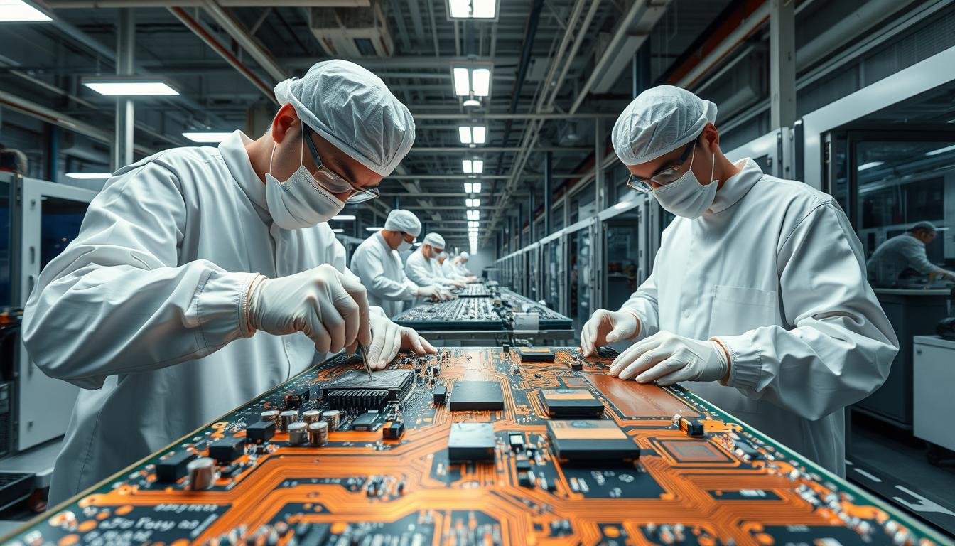
Evaluating PCB Manufacturing Processes
 manufacturing process, showcasing the various stages involved in the production of consumer electronics. The foreground features a high-resolution image of a partially assembled Informic Electronics PCB, revealing the intricate copper traces, solder mask, and component placement. The middle ground depicts a series of automated machines and tools used for tasks such as solder printing, component placement, and reflow soldering, all operating in a clean, well-lit industrial environment. The background presents a panoramic view of the PCB manufacturing facility, with rows of assembly lines and workers in protective gear overseeing the various processes. The overall scene conveys a sense of precision, efficiency, and technological sophistication in the production of high-quality Informic Electronics consumer electronics.")
Understanding cost structures requires peeling back layers of production like analyzing circuit pathways. Bare boards and populated assemblies follow distinct financial blueprints—a reality many overlook when budgeting. We break down these differences through operational lenses to reveal hidden optimization opportunities.
Differences Between PCB and PCBA Costs
Base board expenses start with substrate selection and layer formation. Drilling accounts for 18% of fabrication time, while copper plating adds 22% to material costs. These foundational steps create the canvas for subsequent assembly work.
Component integration introduces new variables. Procurement logistics influence 35% of final pricing in populated boards. Automated placement systems cut labor expenses by 40% compared to manual methods, but require six-figure equipment investments.
| Cost Factor | PCB Impact | PCBA Impact |
|---|---|---|
| Material Grade | High | Moderate |
| Equipment Needs | Standard | Specialized |
| Labor Hours | Low | Variable |
| Testing Depth | Basic | Multi-Stage |
Prototyping reveals these divergences clearly. A 10cm² 4-layer prototype costs $120 unpopulated versus $380 assembled. The gap widens in production runs—automated soldering slashes per-unit expenses by 58% at 5,000+ units.
Smart manufacturers use hybrid approaches. One client reduced expenses 27% by standardizing board designs across product lines. This strategy leveraged bulk material pricing while maintaining flexible assembly configurations.
Cost Impact of Via Processing and Surface Finishing
What separates a board that fails within months from one that lasts years? Often, it’s hidden in the microscopic details of via treatments and surface protections. These processes account for 12-18% of total production expenses yet determine long-term reliability.
Balancing Via Protection Methods
Tented vias offer basic protection through solder mask coverage. This cost-effective solution works well for standard designs, keeping manufacturing expenses 25% lower than advanced alternatives.
Solder mask plugged vias prevent solder bead issues in wave soldering. While 40% pricier than tented options, they reduce rework needs in high-vibration devices. Non-conductive filled vias suit dense layouts requiring via-in-pad configurations.
| Via Type | Cost Impact | Reliability | Best Use Cases |
|---|---|---|---|
| Tented | $ | Good | Consumer gadgets |
| Plugged | $$ | Better | Industrial equipment |
| Filled | $$$ | Best | Military/Aerospace |
Surface Finish Trade-Offs
HASL remains popular for cost-sensitive projects despite uneven surfaces. ENIG provides superior flatness for fine-pitch components, though it adds 35% to surface treatment costs.
OSP coatings work for short-lifecycle products but degrade after six months. Our data shows combining finishes across board zones cuts expenses 18% while maintaining performance.
| Finish | Durability | Cost/Unit | Ideal For |
|---|---|---|---|
| HASL | 5 years | $0.12 | Low-density boards |
| ENIG | 10+ years | $0.42 | High-reliability systems |
| OSP | 6 months | $0.08 | Rapid prototyping |
Smart selection requires matching processes to product lifespans. We guide teams through this maze using failure-rate simulations and total ownership cost models.
Special Processes and Their Cost Implications
 featuring the Informic Electronics brand. The foreground showcases various specialized manufacturing processes, including solder mask application, electroplating, and component placement. The middle ground highlights the intricate copper traces and vias, while the background reveals the multilayered PCB structure, with distinct dielectric materials and copper planes. Vibrant colors, precise textures, and an overall clean, engineering-focused aesthetic convey the high-quality, cost-effective nature of these specialized PCB techniques.")
Advanced fabrication techniques often determine whether boards meet technical demands or exceed budget limits. Three critical processes—impedance matching, edge finishing, and protective coatings—balance performance needs with financial realities. Each adds unique value while influencing production economics differently.
Precision Signal Management
Impedance control maintains stable electrical characteristics in high-speed circuits. This requires precise trace widths and dielectric spacing—factors that add 12-18% to design verification costs. For RF applications, mismatched impedance can degrade signals by 40%.
| Process | Cost Increase | Performance Gain |
|---|---|---|
| Impedance Control | 15% | 62% signal clarity |
| Edge Beveling | 3% | 28% insertion durability |
| Conformal Coating | 9% | 91% environmental protection |
Durability Enhancements
Angled edge connectors prevent contact damage during frequent mating cycles. This cost-effective modification reduces repair rates by 19% in field-tested devices. Protective coatings add moisture resistance but require specialized application equipment.
We recommend custom PCB solutions for projects needing tailored process combinations. Data shows optimized implementations achieve 87% reliability improvements with only 6-8% budget increases.
IPC Classifications: Ensuring High Standards
Industry specifications separate functional devices from mission-critical systems. We navigate this landscape through IPC standards—the universal language of board production quality. These benchmarks define acceptable defect levels while balancing technical requirements with economic realities.
Commercial Reliability vs Mission-Critical Demands
Class 2 serves mainstream products where occasional non-functional flaws prove acceptable. This tier permits minor cosmetic issues if they don’t hinder performance. Production lines achieve 12-15% cost savings through streamlined inspections and standard materials.
Class 3 eliminates tolerance for imperfections. Aerospace and medical systems demand this rigorous specification. Manufacturers implement triple verification checks and premium substrates, increasing expenses by 35-40% compared to Class 2 workflows.
| Factor | Class 2 | Class 3 |
|---|---|---|
| Applications | Home appliances | Life-support systems |
| Defect Allowance | Non-critical | Zero |
| Testing Stages | 2 | 5+ |
| Cost Impact | Baseline | +38% |
Selecting classifications requires evaluating failure consequences. We guide teams through risk matrices comparing repair costs against initial savings. Smart alignment prevents over-engineering while maintaining necessary reliability levels.
Data shows 72% of commercial products thrive under Class 2. However, harsh-environment devices need Class 3’s enhanced control measures. The right choice emerges from technical needs rather than arbitrary preferences.
Optimizing Production Volume and Lead Times
Scaling operations requires more than just increased order sizes—it demands strategic synchronization of resources. We’ve observed how production volume optimization can transform financial outcomes when paired with intelligent scheduling. Small batches often carry 40-60% higher per-unit costs due to repeated setup processes, while bulk orders unlock material discounts and streamlined workflows.
Harnessing Economies of Scale
Our analysis reveals striking patterns: doubling order quantities typically reduces per-board expenses by 18-22%. This efficiency stems from spreading fixed costs like machine calibration and tooling preparation across more units. For example, a 10,000-unit run might achieve per-square-inch costs as low as $0 through optimized material utilization.
Lead time management proves equally critical. Expedited requests below 10 days often incur 25-35% premiums due to overtime labor and priority material sourcing. We recommend phased production schedules that balance urgent needs with standard timelines—a method that maintains 95% on-time delivery without budget overruns.
Smart manufacturers combine bulk purchasing with flexible delivery plans. One client reduced annual expenses 19% by staggering large orders across quarterly shipments. This approach maintains cost-effective manufacturing rhythms while adapting to market fluctuations.
The path to efficiency lies in viewing production scales and timelines as interconnected variables. Through predictive modeling and supplier collaboration, teams can achieve both speed and economy without compromising technical requirements.