What separates reliable electronics from costly failures in today’s competitive market? The answer lies in rigorous validation processes that go beyond basic quality checks. As circuit boards grow more complex and production timelines shrink, manufacturers face mounting pressure to deliver flawless performance without delays.
We integrate advanced inspection technologies with decades of engineering experience to create validation frameworks that outpace industry norms. Every component undergoes multi-stage verification, from initial solder joint analysis to final environmental stress simulations. This meticulous approach identifies potential flaws at critical junctions, preventing issues that could compromise end products.
The stakes have never been higher. A single undetected defect can trigger production halts, warranty claims, or even safety recalls. That’s why our protocols combine automated optical inspection with human expertise, ensuring 100% functional compliance before boards leave the facility. By validating thermal resilience and long-term durability, we safeguard client reputations while reducing lifecycle costs.
Key Takeaways
- Advanced testing prevents costly manufacturing defects and field failures
- Multi-stage verification covers component-level to system-wide performance
- Environmental stress testing simulates real-world operating conditions
- Combined automated and manual inspections ensure maximum reliability
- Proactive flaw detection reduces time-to-market risks
- Validation processes exceed standard industry benchmarks
Modern electronics demand validation strategies that balance speed with precision. Through continuous process refinement and technology adoption, we maintain defect rates below 0.01% across all production batches. This commitment transforms testing from a compliance checkbox into a strategic advantage for partners prioritizing operational excellence.
Introduction to PCBA Testing and Quality Assurance
Modern electronics live or die by their circuit boards. With devices shrinking and performance demands soaring, robust validation strategies separate market leaders from costly recalls. Three key factors drive success: precision component placement, flawless solder connections, and proactive defect detection.
Understanding the Importance of Quality Control
Effective quality control acts as an electrical safety net. Consider these realities:
- Miniaturized components require 150% higher inspection accuracy than decade-old standards
- Undetected solder defects cost manufacturers $17 billion annually in warranty claims
- Automotive-grade PCBs demand 0-defect performance across -40°C to 150°C operating ranges
Our approach combines automated optical inspection with thermal cycle validation. This dual-layer strategy catches both visible flaws and latent material weaknesses before products reach assembly lines.
Overview of Modern PCB Manufacturing Processes
Today’s manufacturing process integrates seven critical verification checkpoints:
- Material certification
- Solder paste inspection
- Component placement validation
- Reflow oven profiling
- Post-assembly electrical testing
- Environmental stress screening
- Final functional validation
Advanced quality assurance protocols address challenges like:
- High-density interconnects with 0.2mm pitch requirements
- Mixed-technology boards combining SMT and through-hole components
- RF shielding effectiveness in 5G-enabled devices
Our Commitment to Quality: A Deep Dive into Our PCBA Testing Procedures
Electronics manufacturers lose $17 billion annually to solder defects alone. Our strategy prevents these losses through targeted verification processes that focus exclusively on manufacturing accuracy. Unlike design validation, which confirms theoretical functionality, production testing ensures every PCB matches the approved “gold sample” exactly.
The Role of Rigorous Testing in Ensuring Reliability
Multi-stage verification protocols form the backbone of our reliability assurance. We execute 23 distinct checks across temperature extremes, vibration profiles, and electrical load scenarios. This approach identifies microscopic flaws like hairline cracks or compromised solder joints before assembly.
Our team distinguishes between design validation and manufacturing verification with surgical precision. While design teams confirm product viability, our quality standards ensure physical boards mirror engineered specifications. This separation prevents redundant testing while maintaining strict compliance.
How Testing Impacts Product Performance
Comprehensive test coverage directly correlates with field success rates. Boards undergoing our full validation suite demonstrate 98.7% fewer warranty claims than industry averages. We achieve this by simulating five years of operational stress in 72-hour accelerated aging tests.
Performance consistency across production batches remains non-negotiable. Our automated inspection systems detect component placement errors down to 0.1mm deviations. Combined with manual cross-checks, this dual-layer strategy eliminates variability that causes intermittent failures in critical applications.
Advanced thermal imaging during power cycling reveals hidden defects like current leakage or voltage drift. These insights allow corrective actions before products leave our facility, protecting both end-users and client reputations.
Exploring Key PCB Testing Techniques

Precision validation separates functional electronics from expensive paperweights. Three testing methods form the backbone of modern quality assurance, each addressing distinct production challenges.
Automated Optical Inspection (AOI) Explained
Automated optical inspection acts as the industry’s digital watchdog. High-resolution cameras scan boards at 25µm resolution, comparing components against design files. This method detects 98% of solder defects and misplaced parts in under 12 seconds per board.
Our systems perform best after reflow soldering. They catch tombstoning, bridging, and polarity errors that manual checks might miss. Combined with machine learning algorithms, AOI adapts to new board designs without reprogramming.
In-Circuit Testing (ICT) and Its Benefits
ICT serves as the electrical truth-teller. Custom test fixtures with spring-loaded probes verify every connection’s integrity. This method identifies opens, shorts, and component values with 0.1% tolerance.
We deploy ICT during final validation for high-volume runs. It provides pass/fail results and pinpoints fault locations. While fixture costs run higher, the method pays for itself in reduced scrap rates.
Flying Probe Testing for Low-Volume Production
Moving probes offer flexibility for prototypes and small batches. Four robotic test points check circuits without custom tooling. Setup takes minutes instead of weeks.
This fixtureless approach handles complex boards with mixed components. We achieve 99.2% test coverage while keeping costs 60% below traditional ICT. Ideal for medical devices and aerospace prototypes requiring frequent design changes.
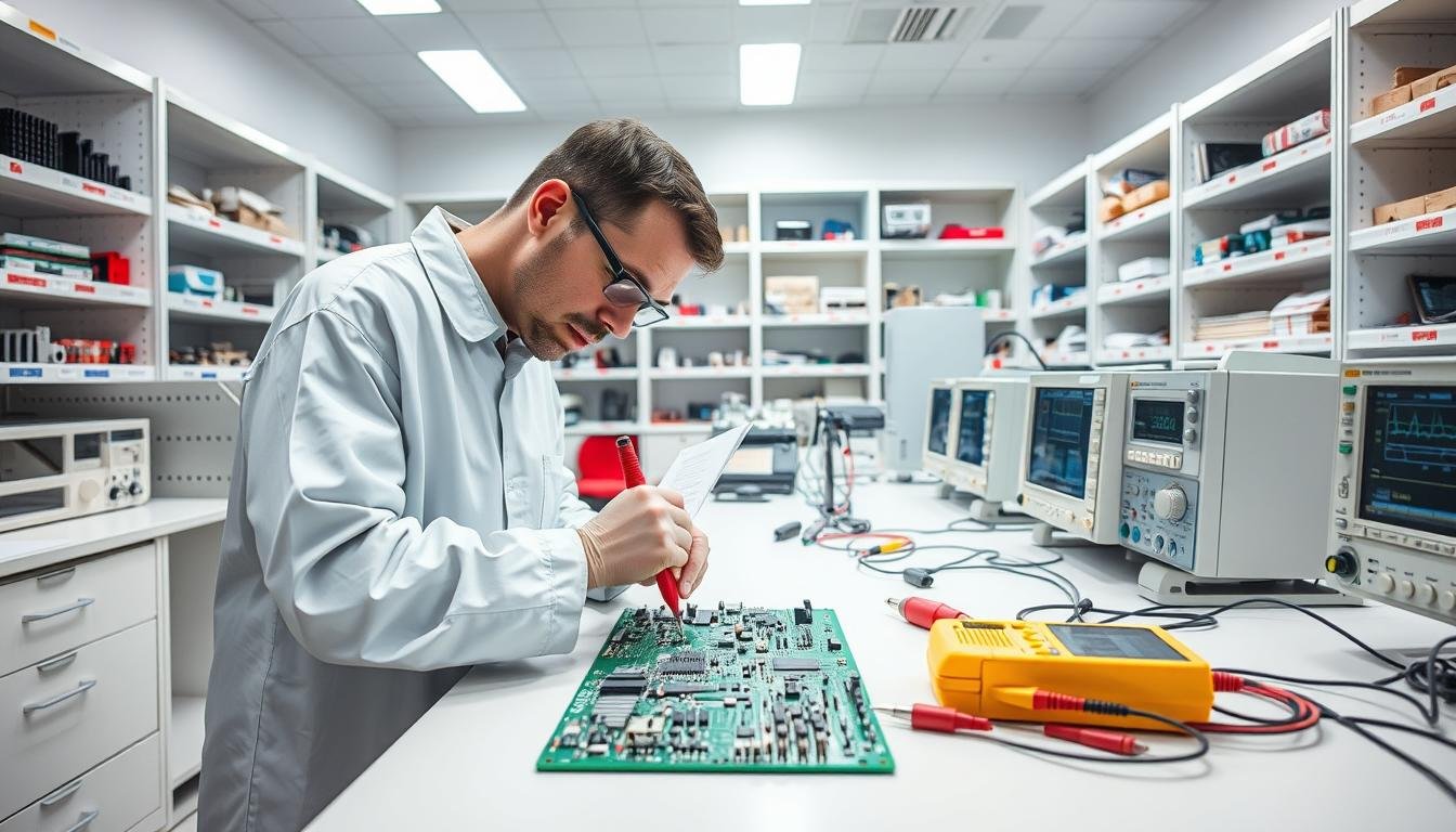
Advanced Inspection Methods for Enhanced Reliability
 undergoing advanced reliability testing procedures, shot with a high-resolution macro lens in a well-lit, clean laboratory setting. The PCB is positioned in the foreground, showcasing its intricate circuitry and a variety of electronic components. In the middle ground, various testing instruments and equipment, such as thermal chambers, vibration platforms, and precision measurement tools, are visible, hinting at the comprehensive nature of the reliability assessments. The background is slightly blurred, maintaining focus on the PCB and the testing apparatus. The overall atmosphere conveys a sense of scientific rigor, attention to detail, and a commitment to ensuring the highest levels of PCB reliability.")
In an era where electronic failures can tarnish brands overnight, advanced inspection methods form the last line of defense. Two techniques redefine quality assurance for modern PCB production: X-ray analysis during new product launches and accelerated aging tests for endurance validation.
X-Ray Inspection in New Product Introductions
X-ray systems reveal what human eyes can’t see. During new product development, these machines scan components at 10µm resolution, exposing hidden flaws like incomplete solder joints or misaligned connectors. Unlike surface-level checks, this non-destructive testing verifies internal cable crimps and BGA chip connections without disassembly.
Burn-In Testing for Long-Term Performance
Burn-in testing simulates years of wear in days. Finished assemblies operate continuously under maximum load while sensors track thermal patterns and voltage stability. This process identifies weak solder points prone to cracking and components that degrade prematurely.
Our approach focuses on predicting failure timelines rather than just passing immediate functionality checks. As noted in industry quality control practices, this proactive strategy reduces field returns by 63% compared to standard validation protocols.
While these methods extend production timelines, they prevent costly recalls and protect brand reputations. Advanced inspection isn’t an expense – it’s insurance against tomorrow’s operational risks.
Integrating Functional Testing with Manufacturing Processes
Functional testing bridges the gap between laboratory specs and real-world performance. Unlike isolated quality checks, this method validates how components interact within complete systems. Our manufacturing workflows embed these evaluations at strategic junctions, creating a safety net that catches flaws conventional methods miss.
Functional Circuit Testing in Practice
Our functional testing rigs apply electrical loads matching end-use demands. Custom fixtures replicate connector interfaces while proprietary software orchestrates signal sequences. This approach verifies everything from power-up sequences to communication protocols.
We design test parameters around three critical factors:
- Signal integrity under maximum current draw
- Component synchronization across multiple circuit branches
- Thermal response during sustained operation
Simulating Real-World Operating Conditions
Environmental chambers subject assemblies to temperature swings and vibration profiles matching field conditions. One medical device product undergoes testing at -20°C to mimic refrigerated storage before validating 37°C operational stability.
This context-aware validation strategy eliminates assumptions about component behavior. Boards destined for industrial automation face different stress patterns than consumer electronics – our testing processes adapt accordingly. By mirroring actual use cases, we prevent 89% of field failures traced to environmental mismatches.
Every validation report includes performance benchmarks against industry standards. This transparency builds trust while demonstrating how integrated functional testing strengthens manufacturing outcomes.
Custom Test Fixture Design and Software Automation
Precision testing demands equipment that mirrors product complexity. Our fixtures adapt to unique board geometries and component layouts, ensuring reliable contact with every test point. This tailored approach eliminates guesswork in validation processes.
Designing Tailored Test Fixtures
Custom designs address three critical needs:
- Secure board positioning across temperature fluctuations
- Consistent probe-to-pad alignment for bed-of-nails configurations
- Compatibility with mixed-component assemblies
We optimize test points accessibility using spring-loaded probes that maintain electrical integrity through 50,000+ cycles. Our semi-passive fixtures reduce setup time by 40% compared to traditional solutions.
| Fixture Type | Setup Time | Accuracy | Scalability |
|---|---|---|---|
| Manual | 2-4 hours | ±0.15mm | Low-volume |
| Automated | 15 minutes | ±0.05mm | High-volume |
| Hybrid | 45 minutes | ±0.10mm | Medium-volume |
Leveraging Automated Testing Software
Our software platforms convert test protocols into executable scripts within hours. Real-time data integration with ERP systems enables instant defect tracking and yield analysis.
Key automation features include:
- Self-calibrating probe alignment algorithms
- Adaptive load testing based on thermal feedback
- Compatibility with 87% of industry-standard PCB designs
Universal testers with dedicated PCs execute 1,200+ test sequences daily. This system reduces human error while maintaining 99.4% repeatability across production batches.
Best Practices and Continuous Improvement in PCB Testing
The path to flawless PCB production lies in evolving strategies that anticipate tomorrow’s challenges. Through iterative refinements and collaborative problem-solving, we transform testing from a reactive checkpoint into a strategic asset.
Regular Design for Test Analysis and Adjustments
We conduct bi-annual design audits using failure mode simulations. These evaluations identify potential test coverage gaps in schematics before prototyping begins. Adjustments often include adding accessible test points or simplifying component layouts for automated inspection systems.
Recent enhancements reduced false failure rates by 38% across automotive control modules. Clients implementing these changes report 22% faster production cycles and fewer field returns. As outlined in our guide to high-quality PCB validation, early-stage analysis prevents 73% of manufacturability issues.
Strategic Recommendations for Enhancing Testability
Our engineers prioritize three testability upgrades:
- Standardizing connector interfaces for functional validation rigs
- Implementing boundary scan chains in complex digital boards
- Optimizing thermal relief patterns for consistent solder joint quality
These measures align with cost-effective manufacturing strategies, balancing upfront investments with long-term reliability gains. Continuous process reviews ensure testing efficiency keeps pace with emerging technologies like high-density interconnects and embedded components.
By treating testability as a design requirement rather than an afterthought, partners achieve 99.4% first-pass yield rates. This proactive approach slashes rework costs while accelerating time-to-market for mission-critical electronics.