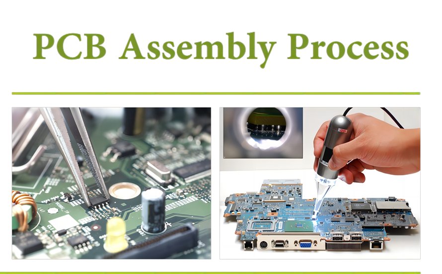
PCB Assembly Process – 8 Main Steps
The PCB assembly process might seem straightforward if you only consider SMT and PTH assembly. However, it involves many detailed steps and supportive processes that ensure high-quality printed circuit assembly.

Get a free quote now!
Step 1: Prepare Files for PCB Assembly
The first and most critical step in the PCB assembly process is preparing the necessary files. These include a Design for Assembly (DFA) check for Gerber files, Bill of Materials (BOM), and production files that our equipment and team will use for assembly.
Gerber files are essential for the assembly process, as they contain the patterns for copper layers, solder masks, and component notations. These files are also necessary for SMT stencil creation and DFA checks. BOM and Pick & Place files provide the component details, such as manufacturer, part number, and placement coordinates, which help ensure accuracy during assembly.
This step identifies potential issues in the design before production begins. It ensures that component dimensions match PCB pads and flags obsolete or incorrect components, minimizing production errors.
After resolving any engineering questions, a production file is created. This file outlines all the details needed for each step of the assembly process, such as incoming material quality control (IQC) requirements, solder paste types, and special processes like conformal coating.
Step 2: SMT Assembly
Once all necessary documents and tools are prepared, the SMT assembly process begins.
Before starting, an SMT stencil must be laser cut to achieve the best results in solder paste application. The stencil size and thickness vary depending on the PCB design.
These files guide the placement of components on the PCB. High-quality assembly requires precise files to ensure accurate placement by the Pick & Place machine.
After preparing the materials, solder paste is applied to the PCB through the stencil. The solder paste quality is critical, so we use trusted brands to ensure top-quality results.
Components are placed on the PCB using high-speed, high-accuracy machines. IPQC (In-Process Quality Control) ensures proper solder paste application and component placement.
Once components are placed, the PCBs go through a reflow oven to solder the components to the board.
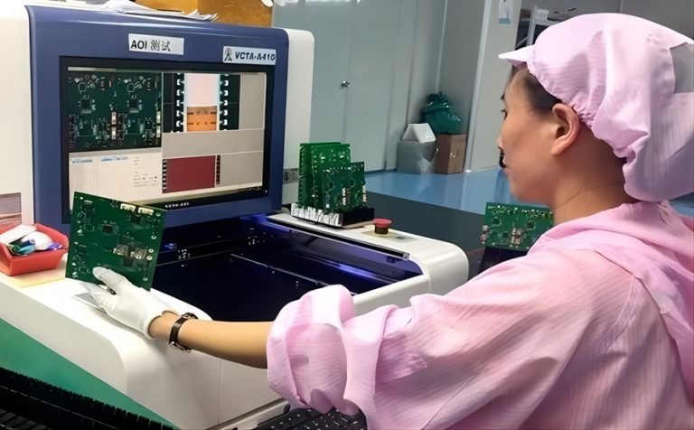
Automatic Optical Inspection (AOI) is used to check for any visual defects. This automated process ensures higher accuracy than manual inspections.
To avoid production issues, the first assembled PCB is inspected to confirm correct assembly before continuing with the production run.
Step 3: PTH Assembly
These are necessary to support the PCB during wave soldering, especially for heavier components.
The PCB is run through a wave soldering machine where molten solder adheres to the component pins and PCB holes.
After soldering, any excess component pins are cut to ensure smooth assembly.
After PTH assembly, quality checks ensure that all components are correctly soldered, preventing defects such as shorts or open circuits.
Step 4: Manual Assembly
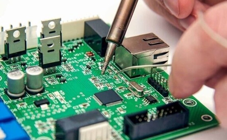
Some components may require manual soldering. This process involves skilled workers using soldering irons to place components where machines cannot. Although manual assembly is less efficient than automated processes, it is sometimes necessary for specific projects.

Step 5: Functional Testing
When all the components are assembled on the PCB, the PCB assembly company will perform functional testing (FCT) if requested by the customer. Functional testing verifies that the assembled PCB functions as expected under real-world conditions. It ensures that the electronic components and the entire PCB work as intended.
A testing fixture is often required to test the PCB’s functionality, and it can be supplied by the customer or created by the PCB assembly company based on the customer’s testing process and specifications. Sometimes, the PCB may need programming or firmware installation into memory chips before the functional testing can proceed. This step ensures that the PCB assembly is fully operational and meets the required performance standards.
During functional testing, engineers may simulate the operating environment of the PCB, checking for potential issues such as power fluctuations, signal integrity problems, and overall stability. Any malfunctioning components or soldering defects discovered during testing are repaired or replaced to meet the quality standards of the final product.
Step 6: Conformal Coating
After passing all tests, conformal coating is applied to the PCBs when required. Conformal coating involves covering the PCB with a protective chemical layer that safeguards the board from moisture, dust, chemicals, and extreme temperatures, ensuring a longer lifespan for the electronic components.
The conformal coating can be applied through various methods, such as dipping, brushing, or spraying, depending on the specific needs of the project. This step is crucial for PCBs that will be used in harsh environments, such as industrial equipment or outdoor electronics.


Step 7: Final Quality Inspection
Once functional testing and conformal coating are complete, a final quality inspection is conducted to ensure that the assembled PCB meets all customer specifications and industry standards. This includes checking for any visible defects, ensuring that all components are correctly placed and soldered, and verifying that the PCB passes all necessary electrical and functional tests.
The final quality inspection may involve visual checks, automated optical inspections (AOI), and manual tests by experienced quality control staff. The goal is to ensure that the finished product is of the highest quality before shipment.
Step 8: Packaging and Shipment
The final step in the PCB assembly process is packaging and shipping the assembled boards to the customer. Proper packaging is essential to protect the PCBs from damage during transit. Anti-static bags, bubble wrap, and custom packaging materials are often used to prevent static discharge, moisture, or physical impact from damaging the boards.
After the boards are securely packaged, they are shipped to the customer, who can then integrate them into their final product. Whether the customer needs small prototypes or large-scale production runs, ensuring that the PCBs arrive in perfect condition is the last critical step in delivering high-quality PCB assembly services.
