Designing printed circuit board assemblies (PCBA) for power electronics presents unique challenges that go beyond standard PCB design practices. These specialized PCBAs must safely handle high voltages and currents while managing thermal issues, ensuring insulation integrity, and meeting stringent safety standards. Whether you’re developing electric vehicle inverters, industrial motor drives, or renewable energy systems, understanding the critical aspects of PCBA for power electronics is essential for creating reliable, efficient, and safe products.
Key Challenges in Power Electronics PCBA Design
Power electronics PCBAs face several critical challenges that must be addressed through careful design and material selection. These challenges directly impact the reliability, safety, and performance of the final product.
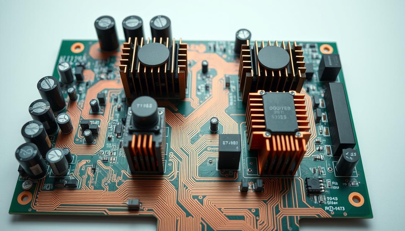
Modern PCBA for power electronics with thick copper traces and thermal management features
High Current Handling Requirements
Power electronics circuits often carry currents ranging from tens to hundreds of amperes. Standard PCB traces designed for signal integrity cannot handle these current levels without excessive heating. The primary challenges include:
- Determining appropriate trace widths to handle high currents without overheating
- Managing voltage drops across traces that can affect circuit performance
- Preventing thermal stress that can lead to delamination or solder joint failure
- Designing for surge currents that may temporarily exceed normal operating levels
Thermal Management Complexities
Power dissipation in high-current applications generates significant heat that must be effectively managed to prevent component failure and ensure reliable operation. Key thermal challenges include:
- Identifying and addressing potential hotspots on the PCBA
- Ensuring adequate heat dissipation from power components
- Preventing thermal coupling between heat-sensitive components
- Maintaining acceptable operating temperatures across varying load conditions
High Voltage Isolation Requirements
When designing PCBA for power electronics with high voltage applications, maintaining proper isolation between high and low voltage circuits is critical for safety and functionality:
- Ensuring sufficient creepage and clearance distances based on voltage levels
- Preventing arc formation between conductors at different potentials
- Maintaining isolation between control circuits and power circuits
- Designing for long-term insulation integrity under environmental stresses
Material Selection for Power Electronics PCBAs
The extreme conditions in power electronics applications demand careful selection of PCB materials. The right substrate, copper thickness, and protective coatings significantly impact performance, reliability, and safety.

Common substrate materials used in power electronics PCBAs
Substrate Materials for High-Power Applications
The substrate provides mechanical support and electrical insulation for the PCBA. For power electronics, standard FR-4 may not always be sufficient:
| Substrate Material | Thermal Conductivity (W/m·K) | Temperature Rating (°C) | Key Applications | Advantages |
| FR-4 | 0.3-0.5 | 130-140 | Low to medium power applications | Cost-effective, widely available |
| High-Tg FR-4 | 0.3-0.5 | 170-180 | Medium power applications | Better thermal stability than standard FR-4 |
| Polyimide | 0.3-0.5 | 250-300 | High-temperature applications | Excellent thermal stability |
| Metal Core (Aluminum) | 1.0-2.2 | 150-170 | LED lighting, power converters | Enhanced heat dissipation |
| Ceramic (Al2O3) | 20-30 | 600+ | High-power converters, automotive | Superior thermal performance |
Copper Thickness Considerations
Copper thickness directly affects the current-carrying capacity of PCB traces. For PCBA for power electronics, standard 1 oz/ft² (35 μm) copper is often insufficient:

Cross-section showing different copper thicknesses used in power electronics PCBAs
| Copper Weight | Thickness (μm) | Current Capacity (10°C Rise) | Typical Applications |
| 1 oz/ft² | 35 | 1.0A per mm width | Signal traces, low-power circuits |
| 2 oz/ft² | 70 | 1.8A per mm width | Medium power circuits |
| 3 oz/ft² | 105 | 2.5A per mm width | High-current power supplies |
| 4 oz/ft² | 140 | 3.2A per mm width | Industrial power converters |
| 6 oz/ft² | 210 | 4.5A per mm width | EV power electronics, high-current applications |
Trace Width Calculator for Power Electronics
Calculate the optimal trace width for your power electronics application based on current requirements, copper thickness, and acceptable temperature rise.
Protective Coatings and Conformal Coatings
In high-voltage and harsh environment applications, protective coatings provide an additional layer of insulation and environmental protection:
- Acrylic conformal coatings – Good moisture resistance, easy to apply and repair, suitable for moderate voltage applications
- Silicone conformal coatings – Excellent temperature resistance (-65°C to +200°C), good for high-temperature power electronics
- Polyurethane coatings – Superior chemical and abrasion resistance, ideal for harsh industrial environments
- Parylene coatings – Excellent dielectric properties and moisture barrier, perfect for high-voltage applications
- Epoxy coatings – Excellent chemical and moisture resistance, provides mechanical protection
Thermal Management Strategies for PCBA in Power Electronics
Effective thermal management is critical for the reliability and performance of PCBA for power electronics. High current flow generates significant heat that must be dissipated to prevent component failure and ensure long-term reliability.

Thermal management techniques implemented in power electronics PCBA design
Component Placement for Optimal Thermal Performance
Strategic component placement is the first step in effective thermal management for power electronics PCBAs:
- Distribute heat-generating components across the board to prevent hotspots
- Place high-power components near board edges or in areas with good airflow
- Maintain adequate spacing between heat-generating components
- Position temperature-sensitive components away from heat sources
- Consider the thermal impact of component orientation and mounting methods
Thermal Vias and Copper Pours
Copper’s excellent thermal conductivity can be leveraged to dissipate heat effectively:

Thermal vias arrangement under a power component to facilitate heat transfer
- Implement thermal vias under heat-generating components to transfer heat to inner or bottom layers
- Use large copper pours connected to ground or power planes for improved heat spreading
- Consider filled or partially filled thermal vias for enhanced thermal conductivity
- Implement star-pattern thermal via arrays under power components
- Use thick copper planes (2 oz or greater) for improved thermal conductivity
Active and Passive Cooling Solutions
Beyond PCB design techniques, additional cooling methods may be necessary for high-power applications:
Passive Cooling
- Heat sinks attached to power components or PCB
- Thermal interface materials to improve heat transfer
- Natural convection cooling through enclosure design
- Phase-change materials for thermal buffering
Active Cooling
- Forced-air cooling with fans or blowers
- Liquid cooling systems for high-power applications
- Thermoelectric coolers for precise temperature control
- Heat pipes for transferring heat to remote heat sinks
Thermal Management Design Guide
Download our comprehensive guide to thermal management techniques for power electronics PCBAs, including detailed design examples and calculation methods.
High-Voltage Design Considerations for PCBA in Power Electronics
Designing PCBA for power electronics applications involving high voltages requires special attention to prevent arcing, ensure proper isolation, and maintain long-term reliability under electrical stress.

High-voltage design features implemented in power electronics PCBA
Creepage and Clearance Requirements
Maintaining proper separation between conductors at different potentials is critical for high-voltage safety:
| Working Voltage (V) | Minimum Clearance (mm) | Minimum Creepage (mm) – PCB Group IIIa | Pollution Degree 2 |
| 0-50 | 0.2 | 0.5 | Indoor controlled environment |
| 51-100 | 0.2 | 0.7 | Indoor controlled environment |
| 101-300 | 0.5 | 1.25 | Indoor controlled environment |
| 301-600 | 1.0 | 2.5 | Indoor controlled environment |
| 601-1000 | 2.0 | 4.0 | Indoor controlled environment |
Key techniques to enhance creepage and clearance include:
- Implementing slots or cutouts in the PCB to increase creepage distance
- Using physical barriers or insulating materials between high-voltage sections
- Designing with rounded copper edges to reduce electric field concentration
- Applying conformal coating to increase effective creepage distance
Arc Prevention Techniques
Preventing arc formation is critical in high-voltage PCBA for power electronics:

Arc prevention techniques implemented in high-voltage PCBA design
- Eliminate sharp points and edges in copper traces and component leads
- Use rounded corners for high-voltage traces to reduce electric field concentration
- Implement guard traces or ground planes around high-voltage sections
- Apply conformal coating with high dielectric strength
- Consider potting or encapsulation for extreme voltage applications
Isolation and Separation Strategies
Proper isolation between high-voltage and low-voltage circuits is essential for safety and functionality:
- Physically separate high-voltage and low-voltage sections on the PCB
- Use optocouplers or digital isolators for signal transfer across isolation barriers
- Implement isolated power supplies for control circuits
- Consider Y-capacitors for EMI suppression across isolation barriers
- Use reinforced insulation for safety-critical applications
High-Voltage PCB Design Checklist
Ensure your high-voltage PCBA designs meet safety and reliability standards with our comprehensive design checklist.
Safety Standards and Compliance for PCBA in Power Electronics
Power electronics PCBAs must comply with various industry standards to ensure safety, reliability, and electromagnetic compatibility. Understanding and implementing these standards is essential for product certification and market acceptance.

Common safety certification marks relevant to power electronics PCBAs
Key Industry Standards for Power Electronics
Several critical standards govern the design and testing of PCBA for power electronics:
| Standard | Description | Key Requirements | Application Areas |
| IPC-2221 | Generic Standard for Printed Board Design | Electrical clearance, creepage distances, conductor sizing | All PCB designs |
| IPC-2152 | Standard for Determining Current-Carrying Capacity in PCBs | Trace width sizing for current capacity | High-current applications |
| UL 60950-1 | Information Technology Equipment Safety | Electrical spacing, insulation, grounding | IT and power supply equipment |
| IEC 61010-1 | Safety Requirements for Electrical Equipment | Protection against electric shock, thermal hazards | Test and measurement equipment |
| IEC 60664-1 | Insulation Coordination for Equipment | Clearance, creepage distances, solid insulation | Low-voltage systems |
Testing Protocols for Power Electronics PCBAs
Comprehensive testing is essential to verify the safety and reliability of power electronics PCBAs:

Safety testing of power electronics PCBA in a certification laboratory
- Hipot Testing – Verifies insulation integrity by applying high voltage between isolated circuits
- Insulation Resistance Testing – Measures resistance between isolated circuits
- Thermal Cycling – Evaluates performance under temperature extremes
- Power Cycling – Tests reliability under repeated power on/off cycles
- EMC Testing – Verifies electromagnetic compatibility
- Environmental Testing – Evaluates performance under humidity, vibration, and shock
Documentation Requirements
Proper documentation is essential for compliance and traceability:
- Detailed design documentation including creepage and clearance calculations
- Material declarations and certificates for all components
- Test reports and certification documentation
- Risk assessment and safety analysis documentation
- Manufacturing process documentation and quality control procedures
Real-World Applications of PCBA for Power Electronics
Power electronics PCBAs are essential components in numerous applications across various industries. Understanding how these specialized PCBAs are implemented in real-world systems provides valuable insights for designers and engineers.
Electric Vehicle Power Converters
Electric vehicles rely heavily on power electronics for efficient energy conversion and motor control:

Power electronics PCBA used in an electric vehicle inverter system
- DC-DC Converters – Convert high-voltage battery power to lower voltages for vehicle systems
- Inverters – Convert DC battery power to AC for electric motor drive
- On-board Chargers – Convert AC grid power to DC for battery charging
- Battery Management Systems – Monitor and control battery cells
EV power electronics PCBAs face unique challenges including high voltage (up to 800V), high current (hundreds of amperes), extreme temperature variations, and vibration. These PCBAs typically utilize thick copper (4-6 oz), ceramic or metal-core substrates, and advanced thermal management techniques.
Renewable Energy Systems
Solar inverters and wind power converters rely on specialized power electronics PCBAs:

Power electronics PCBA used in a solar inverter system
- Solar Inverters – Convert DC from solar panels to AC for grid connection
- Maximum Power Point Trackers – Optimize solar panel output
- Wind Power Converters – Convert variable frequency AC to grid-compatible AC
- Energy Storage Interfaces – Manage power flow to/from battery systems
Renewable energy PCBAs must handle high voltage, maintain high efficiency, and operate reliably in outdoor environments. These designs typically incorporate reinforced insulation, conformal coating for environmental protection, and sophisticated thermal management.
Industrial Motor Drives
Industrial motor drives use power electronics PCBAs to control motor speed and torque:

Power electronics PCBA used in an industrial motor drive system
- Variable Frequency Drives – Control AC motor speed by varying frequency
- Servo Drives – Provide precise position and speed control
- Soft Starters – Reduce inrush current during motor startup
- Regenerative Drives – Recover braking energy
Industrial motor drive PCBAs must handle high power levels while maintaining reliability in harsh industrial environments. These designs typically use thick copper layers, robust isolation between power and control sections, and industrial-grade components rated for extended temperature ranges.
Power Electronics PCBA Design Consultation
Need expert guidance for your power electronics PCBA project? Our team of specialists can help with design review, thermal analysis, and safety compliance.
Design Best Practices for PCBA in Power Electronics
Implementing proven design practices is essential for creating reliable, efficient, and safe power electronics PCBAs. These guidelines address the unique challenges of high voltage and high current applications.

Implementation of best practices in power electronics PCBA design
Component Selection and Placement
Careful component selection and strategic placement are fundamental to power electronics PCBA design:
- Select components with appropriate voltage, current, and temperature ratings with adequate safety margins
- Use components specifically designed for power applications (power MOSFETs, high-current inductors, etc.)
- Distribute heat-generating components to prevent hotspots
- Place sensitive control components away from noise sources and heat-generating components
- Orient components to optimize current flow and minimize loop areas
- Consider mechanical stress and vibration when placing large or heavy components
Trace Routing and Power Plane Design
Proper trace routing is critical for current handling and thermal management:

Trace routing techniques for high-current paths in power electronics PCBA
- Size traces according to current requirements using IPC-2152 standards
- Minimize the length of high-current paths to reduce resistance and inductance
- Use multiple vias for high-current paths between layers
- Implement solid copper pours for power and ground planes
- Consider using bus bars for extremely high currents (>50A)
- Route sensitive signal traces away from high-current and high-frequency paths
EMI/EMC Considerations
Electromagnetic interference (EMI) management is essential in power electronics PCBAs:
- Minimize loop areas in high di/dt circuits to reduce radiated emissions
- Use ground planes to provide low-impedance return paths
- Implement EMI filters at power input and output connections
- Use shielding techniques for sensitive circuits or high-frequency sections
- Apply proper grounding techniques, separating power and signal grounds when necessary
- Consider component placement to minimize coupling between circuits
Design for Manufacturability and Testing
Ensuring that power electronics PCBAs can be reliably manufactured and tested is critical:
- Consider fabrication limitations for thick copper PCBs (minimum trace/space, etching capabilities)
- Design for automated assembly where possible, considering pick-and-place and soldering requirements
- Include test points for critical measurements and in-circuit testing
- Implement design for testability features (boundary scan, built-in self-test)
- Consider thermal relief patterns for large copper areas to facilitate soldering
- Include fiducial marks for automated assembly alignment
Advanced Solutions for PCBA in Power Electronics
As power electronics applications demand higher power density, efficiency, and reliability, advanced PCBA technologies are emerging to meet these challenges. These innovative approaches offer significant advantages over traditional designs.
Traditional vs. Advanced PCBA Technologies
Understanding the differences between traditional and advanced approaches helps in selecting the most appropriate technology for specific applications:
| Feature | Traditional Approach | Advanced Solution | Key Benefits |
| Substrate Material | FR-4, High-Tg FR-4 | Ceramic, AlN, Silicon Nitride | 10-20x better thermal conductivity, higher temperature operation |
| Copper Thickness | 1-4 oz copper foil | Thick copper inlay, copper coin technology | Higher current capacity, better thermal performance, reduced thickness |
| Component Mounting | Surface mount, through-hole | Embedded components, chip-on-board | Reduced parasitics, better thermal coupling, smaller footprint |
| Interconnection | Solder joints, vias | Sintered joints, direct bonded copper | Higher temperature operation, better reliability, lower thermal resistance |
| Cooling Method | Heat sinks, forced air | Integrated liquid cooling, phase change materials | Higher cooling capacity, more uniform temperature distribution |
Embedded Component Technology
Embedding components within the PCB substrate offers significant advantages for power electronics applications:

Cross-section of embedded component technology in power electronics PCBA
- Reduced parasitic inductance and resistance through shorter interconnections
- Improved thermal performance with direct coupling to thermal planes
- Higher power density through three-dimensional integration
- Enhanced reliability with protected components
- Reduced EMI through shorter current loops and better shielding
Direct Bonded Copper and Active Metal Brazing
Advanced substrate technologies enable superior thermal performance:

Direct bonded copper (DBC) substrate used in high-performance power electronics PCBA
- Direct Bonded Copper (DBC) – Copper directly bonded to ceramic substrates (Al2O3, AlN)
- Active Metal Brazing (AMB) – Similar to DBC but with higher temperature capability
- Insulated Metal Substrate (IMS) – Metal base with thin dielectric layer and copper circuit layer
- Benefits include excellent thermal conductivity, high voltage isolation, and CTE matching
3D Packaging and Integration
Three-dimensional integration techniques offer new possibilities for power electronics PCBAs:
- Stacked PCB structures with integrated cooling
- Power modules with integrated gate drivers and sensors
- System-in-package solutions combining power and control functions
- Additive manufacturing techniques for complex 3D structures
Advanced PCBA Technologies Webinar
Join our upcoming webinar on advanced PCBA technologies for power electronics applications. Learn about the latest innovations and how to implement them in your designs.
Frequently Asked Questions About PCBA for Power Electronics
What is the minimum creepage distance for 1kV PCBA?
For a 1kV PCBA operating in pollution degree 2 environments (typical indoor controlled environments) using standard FR-4 material (Material Group IIIa), the minimum creepage distance according to IEC 60664-1 is 4.0mm. This distance may need to be increased for applications in higher pollution environments or reduced for specially coated boards. Always consult the specific standard relevant to your application and consider safety margins in your design.
How do I calculate the appropriate trace width for high-current applications?
Trace width for high-current applications should be calculated based on the IPC-2152 standard, which provides charts and formulas for determining trace width based on current, acceptable temperature rise, copper thickness, and trace length. For a quick estimation, a 10A current with a 10°C temperature rise requires approximately 2.5mm (100 mil) width for 1oz copper. For higher currents, consider using copper pours, multiple layers in parallel, or external bus bars. Online calculators based on IPC-2152 are available to simplify this calculation.
What are the best substrate materials for high-temperature power electronics?
For high-temperature power electronics applications (>150°C), ceramic-based substrates are typically the best choice. Aluminum Nitride (AlN) offers excellent thermal conductivity (170-200 W/m·K) and can operate at temperatures up to 900°C. Silicon Nitride (Si3N4) provides superior mechanical strength and thermal shock resistance. Aluminum Oxide (Al2O3) is a more cost-effective option with moderate thermal performance. Polyimide-based PCBs can handle temperatures up to 250-300°C for less demanding applications. The selection should balance thermal performance, electrical properties, mechanical requirements, and cost considerations.
How can I improve thermal management in my power electronics PCBA?
Improving thermal management in power electronics PCBAs involves multiple strategies: 1) Use thicker copper layers (2-4oz or more) for better heat spreading; 2) Implement thermal vias under hot components to transfer heat to inner or bottom layers; 3) Consider metal-core or ceramic substrates for superior thermal conductivity; 4) Strategically place components to distribute heat generation and prevent hotspots; 5) Use thermal interface materials to improve heat transfer to heat sinks; 6) Implement active cooling solutions for high-power applications; 7) Design copper pours with thermal relief connections to facilitate soldering while maintaining thermal conductivity; 8) Consider embedded component technology for improved thermal coupling.
What safety standards must be followed for PCBA in power electronics?
Power electronics PCBAs must comply with several safety standards depending on the application and region. Key standards include: IPC-2221 for general PCB design guidelines; IPC-2152 for current-carrying capacity; UL 60950-1 or IEC 62368-1 for information technology equipment; IEC 61010-1 for measurement and control equipment; IEC 60664-1 for insulation coordination; IEC 60747 for semiconductor devices; and IEC 61800 for adjustable speed electrical power drive systems. Additionally, industry-specific standards may apply, such as ISO 26262 for automotive applications or IEC 60601 for medical devices. Always verify the specific requirements for your target market and application.
Conclusion
Designing PCBA for power electronics applications requires specialized knowledge and careful consideration of unique challenges related to high voltage, high current, and thermal management. By implementing proper material selection, following industry standards, and adopting best design practices, engineers can create reliable and efficient power electronics PCBAs that meet the demanding requirements of modern applications.
As technology advances, new materials and techniques continue to emerge, offering improved performance, higher power density, and enhanced reliability. Staying informed about these developments and understanding when to apply traditional versus advanced solutions is key to successful power electronics PCBA design.
Whether you’re designing for electric vehicles, renewable energy systems, industrial drives, or other power electronics applications, the principles and practices outlined in this article provide a solid foundation for creating PCBAs that can safely and reliably handle high voltage and current requirements.
Need Expert Help With Your Power Electronics PCBA?
Our team of specialists can assist with design review, thermal analysis, component selection, and safety compliance for your power electronics projects.