Have you ever wondered how your smartphone instantly connects you to the world or why your car’s navigation system never loses its way? The answer lies in a hidden hero: the intricate network of components powering every electronic device you use.
At the core of these systems are bare circuit boards transformed into functional powerhouses through precise assembly. Copper pathways – thinner than human hair – create connections between components, turning inert materials into smart devices. This transformation isn’t magic – it’s engineering mastery.
We’ll demystify how blank boards become intelligent systems. First, we explore the critical difference between basic boards and fully operational units. Next, we break down how microscopic electrical pathways enable complex operations. Finally, we reveal why understanding these systems matters for technical professionals and business leaders alike.
Key Takeaways
- Electronic devices rely on assembled boards containing hundreds of microscopic connections
- Copper pathways enable communication between components like processors and sensors
- Component placement accuracy impacts device performance and reliability
- Modern assembly techniques balance precision with mass production demands
- Understanding these systems helps optimize product design and sourcing decisions
Introduction to PCB Assembly and Its Importance
Every modern electronic device pulses with life through a silent conductor – the printed circuit board. These green canvases form the operational backbone of technology, from medical equipment to smart home systems. Their true power emerges when passive boards become active networks through precise component integration.
Understanding the Role of PCBs in Electronics
A blank circuit board resembles a city map without buildings. The fiberglass base acts as land, copper traces as roads, and components as infrastructure. When properly assembled, these elements create working ecosystems where electricity flows like traffic.
Three material layers define every PCB:
- Fiberglass substrate for structural stability
- Copper pathways for signal transmission
- Solder mask insulation preventing electrical shorts
Overview of PCB Assembly versus Bare Board Production
Raw boards become functional through assembly – the process of attaching processors, resistors, and connectors. Think of it as furnishing an empty house: walls exist (bare board), but lights only work when switches connect to wiring (components).
Modern techniques place up to 50,000 parts per hour with microscopic precision. This transformation enables simple boards to execute complex commands – turning on your coffee maker or guiding aircraft.
PCB Design Basics and Material Considerations
 design. The foreground features a detailed view of the copper traces, vias, and pads in a complex, interconnected layout. The middle ground showcases the various insulating layers, including the solder mask and silkscreen, with clear delineation between them. In the background, a subtle grid pattern emerges, representing the base laminate material. Rendered in a muted, technical color palette dominated by shades of green, blue, and copper, the image conveys a sense of precision and engineering prowess. Captured with a shallow depth of field, creating a sense of depth and focus on the intricate PCB design. Branded with the \"Informic Electronics\" logo in the lower right corner.")
Every electronic innovation begins with its architectural foundation – the layered structure determining functionality and durability. We break down these critical elements that transform conceptual designs into operational reality.
Key Components: Substrate, Copper, Solder Mask, and Silkscreen
The substrate forms the board’s backbone, typically using FR4 fiberglass for rigidity. This base material withstands heat during assembly while maintaining dimensional stability.
Thin copper foil layers create conductive pathways through chemical etching. These traces form communication highways between components, with thickness determining current capacity.
Green solder mask does more than color identification. This protective coating prevents accidental contact between copper traces while resisting environmental contaminants.
White silkscreen markings serve dual purposes. Assembly technicians use them for precise component placement, while end-users benefit from diagnostic labels and safety symbols.
Differentiating Rigid, Flexible, and Metal Core PCBs
Rigid FR4 boards dominate consumer electronics due to cost efficiency and proven reliability. Their stable platform suits standard applications from kitchen appliances to office equipment.
Flexible circuits use polyimide films that bend without breaking. Wearable devices and folding smartphones leverage this adaptability, while industrial robotics employ them for moving joints.
Metal core designs prioritize thermal management. An aluminum layer dissipates heat in LED lighting systems and power converters, preventing component failure from excessive temperatures.
Material selection directly impacts performance and cost. Our analysis shows proper layer configuration reduces prototyping errors by 42% in complex designs.
Preparing for Assembly: DFM Checks and Design File Requirements

Success in electronics creation starts long before the first component touches the board. Our teams use pre-production protocols to verify designs against real-world assembly capabilities – a practice that prevents 73% of potential defects according to industry studies.
The Importance of Design for Manufacturability Checks
DFM analysis acts as a technical translator between engineers and assembly teams. We evaluate spacing tolerances, thermal management zones, and material compatibility using proprietary verification tools. Common issues we resolve include trace widths too narrow for current loads and component shadows affecting solder flow.
Three critical areas our checks address:
- Component placement conflicts near board edges
- Inadequate clearance for automated assembly tools
- Copper weight mismatches in high-current paths
Essential Files: Gerber, Drill, and Pick-and-Place Documentation
Precision assembly demands exact digital blueprints. Gerber files (IX274X format) define copper layers with micron-level accuracy, while drill files specify hole locations down to 0.1mm precision. Our systems cross-reference these against your bill of materials to confirm alignment.
Pick-and-place files transform abstract coordinates into machine instructions. These documents tell robotic arms exactly where to position 0201 resistors (smaller than sesame seeds) and QFN chips with 0.4mm lead pitches. Proper file preparation reduces machine calibration time by 40% in our facilities.
PCBA Manufacturing Process: Step-by-Step Guide
Precision defines success in electronics creation. We guide boards through three critical stages that determine device reliability and performance. Each phase combines advanced machinery with material science to achieve microscopic accuracy.
Precision Material Application
The journey begins with solder paste stenciling. A laser-cut stainless steel template aligns perfectly over the board, depositing a SAC305 alloy mixture (96.5% tin, 3% silver, 0.5% copper). This metallic “glue” will later form both electrical and mechanical bonds.
| Solder Type | Composition | Melting Point | Best Use |
|---|---|---|---|
| SAC305 | Sn96.5/Ag3/Cu0.5 | 217°C | Consumer electronics |
| Tin-Lead | Sn63/Pb37 | 183°C | High-reliability systems |
| Bismuth-based | Sn42/Bi58 | 138°C | Heat-sensitive components |
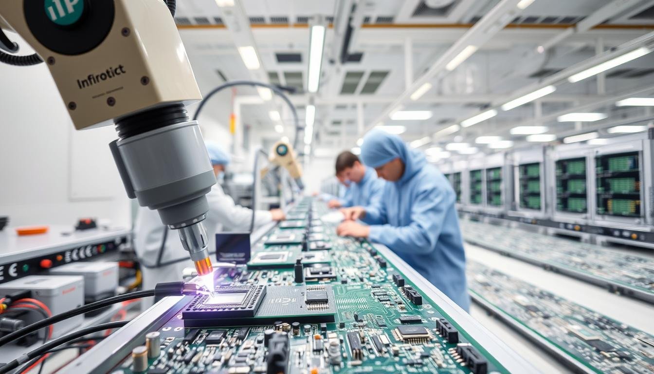
Robotic Component Positioning
Next, vision-guided robots place up to 50 components per second. These machines achieve 0.025mm placement accuracy – thinner than a human hair. Vacuum nozzles handle parts smaller than grain salt without damage.
Modern systems automatically compensate for board warpage and thermal expansion. This ensures perfect alignment even during high-speed operations.
Thermal Bonding Execution
Boards then enter a reflow oven with seven temperature zones. The carefully timed 250°C peak melts solder without harming components. Cooling occurs at 3°C per second to create durable intermetallic bonds.
Double-sided assemblies require special fixturing during second passes. Mechanical clamps and high-tack adhesives prevent existing components from detaching when flipped.
Inspection, Testing, and Quality Control in PCB Assembly
Modern electronics demand flawless operation – a single faulty connection can disable entire systems. We implement rigorous verification protocols to ensure every assembled board meets exact performance criteria before leaving production facilities.
Automated Optical Inspection and X-Ray Methods
Vision systems now handle 98% of defect detection in high-volume production. AOI machines scan boards using 12-megapixel cameras and multi-directional lighting, identifying solder bridges or misplaced components through reflectance patterns.
For complex multilayer designs, X-ray inspection penetrates substrates to reveal hidden flaws. This method detects voids in ball grid arrays (BGAs) and verifies internal via connections invisible to optical systems.
| Method | Detection Capability | Speed | Cost |
|---|---|---|---|
| AOI | Surface defects | 15 sec/board | $$ |
| X-Ray | Subsurface issues | 45 sec/board | $$$ |
| Manual | Obvious errors | 2 min/board | $ |
Functional Testing and Reliability Verification
Final validation involves powering up boards under simulated operating conditions. Our technicians monitor voltage fluctuations, signal integrity, and thermal performance using programmable load testers.
Three critical checks we perform:
- Continuity testing for open/short circuits
- In-circuit testing of individual components
- Burn-in testing at 125% rated capacity
Defective units undergo targeted rework procedures when economically viable. Boards failing multiple tests get scrapped to maintain quality standards – a non-negotiable practice in our facilities.
Regular audits of our manufacturing stages help reduce errors by 37% compared to end-line inspections alone. This proactive approach ensures consistent functionality across production batches while controlling costs.
Through-Hole Component Insertion and Wave Soldering Techniques
While surface-mount technology dominates modern electronics, many designs still require robust mechanical connections only achievable through traditional methods. These legacy techniques maintain relevance in power systems and industrial controls where durability trumps miniaturization.
Human Precision Meets Machine Efficiency
Manual insertion remains vital for large connectors and transformers. Skilled technicians position components using magnified workstations, ensuring proper alignment before securing parts. This hands-on approach handles irregular shapes that challenge automated systems.
Wave soldering automates bulk production for through-hole parts. Boards travel on conveyors through three critical zones:
| Stage | Temperature | Function | Duration |
|---|---|---|---|
| Flux Application | 25°C | Clean surfaces | 12 sec |
| Preheating | 150°C | Activate flux | 90 sec |
| Solder Wave | 260°C | Form joints | 4 sec |
Technical Limitations and Solutions
Double-sided assemblies pose challenges for conventional wave methods. The molten solder bath risks damaging surface-mounted parts on the board’s underside. Selective soldering systems address this by targeting specific areas with focused nozzles.
We verify through-hole connections using cross-sectional analysis and pull-force testing. Proper joints exhibit complete hole fill with concave solder fillets. As one industry expert notes:
“Through-hole reliability often determines product lifespan in harsh environments.”
Modern facilities combine both approaches, using automation where possible while retaining manual stations for specialized components. This hybrid model balances speed with flexibility across mixed-technology designs.
Advanced Production Techniques and Mixed Technology Assembly
Electronics designers increasingly face a critical challenge: integrating microscopic components with heavy-duty parts in single assemblies. This hybrid approach demands technical finesse to balance precision and durability.
Bridging Scale Differences in Component Integration
Surface-mount technology handles components smaller than pencil dots – 01005 resistors and 0.4mm pitch ICs. Through-hole methods secure bulky capacitors and connectors needing mechanical strength. Our teams sequence these processes using strategic assembly processes that prevent thermal damage during multiple soldering phases.
Three key integration strategies ensure success:
- Staged reflow profiles protect heat-sensitive THT parts
- Custom fixturing maintains alignment during board flipping
- Selective solder paste stenciling prevents contamination
Miniaturization pushes component density higher while industrial applications demand robust connections. Our hybrid solutions achieve 99.98% first-pass yield by optimizing machine placement sequences and solder alloy selection. This precision enables smartwatches to survive gym workouts and factory controllers to endure vibration.