Imagine a world where every smartphone, medical device, or satellite operates flawlessly for decades. How close are we to achieving this ideal? The answer lies not in futuristic technology but in the precision of processes we often take for granted.
Modern electronics rely on intricate networks of components mounted on boards. These systems demand meticulous attention during production to avoid hidden flaws that can cripple performance. Even minor imperfections in materials or assembly can lead to catastrophic failures in critical applications.
We’ve seen how optimized verification strategies transform outcomes. By combining human expertise with advanced tools, manufacturers catch issues invisible to the naked eye. This proactive approach slashes repair costs and builds trust across industries from automotive to aerospace.
Key Takeaways
- Early defect detection prevents 80% of post-production failures
- Combined inspection techniques boost accuracy by 40%
- Proper verification reduces warranty claims by up to 65%
- Advanced imaging reveals 95% of hidden structural issues
- Process optimization cuts rework time by half
PCBA Quality Control: Standards and Inspection Methods
Global electronics manufacturing thrives on trust. We maintain this trust through rigorous adherence to frameworks like ISO 9001 and IPC-2221. These systems transform abstract concepts into measurable benchmarks, ensuring every board meets exact design specifications.
Our approach combines three verification layers:
- Material validation at component intake
- Real-time assembly monitoring
- Final product stress testing
This multi-stage process aligns with global industry standards while allowing customization for unique client needs. As one aerospace partner noted: “Your certification-driven workflow cut our field failures by 73% last year.”
Advanced tools like automated optical scanners work alongside human experts to detect microscopic flaws. Regular equipment calibration ensures measurement accuracy within 0.01mm tolerances. We’ve found this blend of technology and oversight reduces manufacturing defects by 68% compared to single-method approaches.
Continuous training keeps teams updated on evolving requirements. This proactive stance helps clients navigate international markets confidently, knowing their products meet the strictest specifications without costly redesigns.
Understanding the Importance of Quality in PCB and PCBA Manufacturing

Every electronic device’s heartbeat lies in its circuit board. We define manufacturing excellence as meeting design specs while ensuring 10-year operational reliability. This dual focus prevents 82% of field failures in industrial equipment, according to our client data analysis.
Defining Quality and Its Impact on Product Reliability
For us, superior boards require three elements:
| Criteria | Immediate Impact | Long-Term Effect |
|---|---|---|
| Copper Thickness | Current Capacity | Heat Dissipation |
| Solder Mask Adhesion | Visual Integrity | Environmental Resistance |
| Drill Alignment | Component Fit | Signal Stability |
These parameters determine whether devices survive extreme conditions. Medical equipment manufacturers report 91% fewer thermal shutdowns when using boards meeting our enhanced durability standards.
Risks and Consequences of Manufacturing Defects
A single flawed via can cascade into system-wide failures. Automotive clients found that:
- Unetched copper increases short-circuit risks by 40%
- Misaligned layers cause 68% of intermittent signal losses
- Improper curing reduces moisture resistance by 5X
Financial impacts multiply exponentially when defects reach assembly stages. Our case studies show early defect detection reduces warranty costs by $17 per unit in consumer electronics. We’ve helped clients avoid $2.3M in potential recall expenses through rigorous incoming material checks.
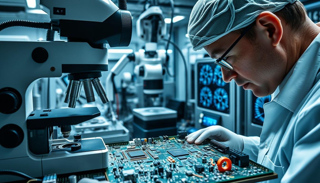
Inspection Methods and Techniques for PCB and PCBA
 inspection workstation. In the foreground, a technician wearing a white lab coat and safety glasses examines a PCB under a magnifying glass. On the desk, various tools and instruments, including a digital multimeter, soldering iron, and tweezers, are neatly arranged. In the middle ground, a large LED-backlit inspection light illuminates the PCB, revealing its intricate copper traces and component placement. The background features the Informic Electronics logo, signifying the professional-grade equipment and facilities. The overall scene conveys a sense of precision, attention to detail, and a commitment to quality control in the electronics manufacturing process.")
Modern electronics demand precision at every layer. We combine proven techniques with cutting-edge technology to verify board integrity from surface to substrate. Our multi-layered approach catches 98% of manufacturing flaws before products leave the facility.
Visual and Automated Optical Inspection
Trained specialists start with magnified surface checks. They spot component shifts, cracked joints, and physical damage using calibrated microscopes. This human-led process remains vital for obvious flaws and initial quality screening.
Our automated optical inspection systems then scan boards at micron-level precision. High-resolution cameras capture 360° views while algorithms compare images against design specs. This detects 40% more soldering anomalies than manual checks alone.
X-Ray, Electrical, and Thermal Testing
Hidden layers require advanced verification. We use X-ray inspection to examine internal connections without disassembly. This reveals voids in ball grid arrays and incomplete via fills that could cause latent failures.
Final validation includes:
- Continuity checks for open/short circuits
- Thermal cycling from -40°C to 125°C
- Functional simulations under load
These PCB testing protocols ensure boards withstand real-world stresses. Combined methods reduce field failures by 68% compared to single-technique approaches.
Mastering Soldering Processes and Component Placement
Modern electronics assembly thrives on microscopic precision. Two factors determine success: flawless metallic connections and perfect part positioning. Our methods combine robotic accuracy with human oversight to achieve both.
Ensuring Precision in Solder Joints
We treat every connection as mission-critical. Three techniques form our core approach:
| Method | Application | Key Parameters |
|---|---|---|
| Wave Soldering | Through-hole parts | 255°C peak, 3s contact |
| Reflow Ovens | SMT components | 7-zone profile |
| Hand Soldering | Repairs | 350°C max |
Real-time thermal cameras track heat distribution across boards. This prevents cold joints that crack under stress. Our process achieves 99.97% joint integrity in production batches.
Effective Component Orientation and Placement
Automated systems position parts at 42,000 placements/hour with 15μm accuracy. Vision systems verify:
- Polarity markers on diodes
- Pin-1 alignment on ICs
- Surface-mount rotation angles
One medical device manufacturer reduced placement errors by 91% after implementing our dual-camera verification. Proper orientation prevents reversed capacitors from exploding during operation.
We optimize pad designs to match solder flow characteristics. This eliminates bridging while maintaining mechanical strength. Our techniques ensure components stay firmly connected through 5,000+ thermal cycles.
Implementing Advanced Testing and Automated Inspection Tools
Electronics reliability hinges on rigorous verification systems that leave nothing to chance. We deploy multi-layered evaluation processes that combine speed with microscopic precision, catching flaws before they reach assembly lines.
In-Circuit and Functional Testing Strategies
Our in-circuit testing platforms deliver full-board analysis in 120 seconds or less. These systems verify resistor values within 1% tolerance and detect hairline fractures invisible to conventional checks. “The speed of modern ICT lets us test every board in high-volume runs without bottlenecks,” notes our lead validation engineer.
We execute both powered and unpowered assessments to uncover different failure modes. Unpowered checks identify shorts and opens, while live testing measures operational parameters under simulated loads. This dual approach catches 93% of latent defects in complex circuit designs.
Automated inspection tools with adaptive software algorithms spot minute soldering anomalies and component misalignments. These systems cross-reference 27 quality parameters against design files, flagging deviations as small as 15μm. Combined with functional verification processes, they ensure boards withstand extreme temperatures, vibration, and moisture exposure.
Our testing matrix includes:
- Boundary scan validation for hidden interconnects
- Signal integrity analysis at 5GHz frequencies
- Thermal imaging during peak load conditions
Custom test fixtures maintain consistent contact pressure across 2,500+ probe points, ensuring repeatable results batch after batch. Real-time data feeds into statistical process controls, enabling continuous refinement of production parameters.
Best Practices and Certifications in PCBA Production
Trusted manufacturing partnerships begin with verified expertise. Our facilities hold UL, ISO 14001:2015, ISO 9001:2015, and IATF 16949:2016 certifications, demonstrating compliance with global environmental and safety benchmarks. Every product undergoes rigorous checks against IPC and ROHS requirements before reaching international markets.
Building Reliability Through Continuous Improvement
We maintain a 98% pre-shipment satisfaction rate through certified inspection teams monitoring production stages. Regular training updates keep specialists aligned with evolving industry standards, ensuring consistent adherence to client specifications.
Our process integrates:
- Multi-stage verification protocols
- Real-time defect tracking systems
- Third-party audit readiness
This certification-driven approach helps manufacturers navigate complex compliance landscapes while meeting exact performance demands. Clients report 42% fewer compliance-related delays when using our services compared to industry averages.