In an industry where innovation races forward, why do technical teams increasingly rely on analyzing existing circuit boards? The answer lies in a process that combines forensic-level precision with strategic problem-solving. Modern electronics demand methods to extend product lifecycles, protect proprietary designs, and decode competitors’ advancements—all while navigating shrinking component availability.
We’ve seen firsthand how systematic circuit board analysis helps manufacturers overcome obsolescence challenges. When original parts vanish from the market, reconstructing designs becomes critical for maintaining operational systems. This approach also safeguards intellectual assets by creating verifiable documentation of legacy products.
The methodology goes beyond simple duplication. Teams must decode layered schematics, identify substitute components, and verify functional equivalence. Success requires specialized tools—from high-resolution imaging systems to advanced simulation software—paired with deep domain knowledge.
Key Takeaways
- Modern electronics depend on precise reconstruction of legacy designs for system continuity
- Component shortages drive demand for accurate circuit board replication strategies
- Protecting intellectual property requires verifiable design documentation processes
- Advanced imaging and simulation tools enable error-free design replication
- Cross-functional expertise ensures functional parity in reconstructed boards
Our experience shows that effective design recovery bridges past innovations with future upgrades. It empowers teams to improve upon original layouts while maintaining compatibility—a vital capability in industries where equipment longevity spans decades.
Introduction to PCB Reverse Engineering
What drives engineers to meticulously dissect and recreate electronic designs? At its core, PCB reverse engineering transforms physical boards into actionable technical insights. This methodical approach reveals how components interact, enabling teams to replicate or improve devices when original blueprints are lost or outdated.
We approach each project through three critical phases: schematic extraction, layout reconstruction, and material analysis. Teams systematically decode component relationships, layer-by-layer, using specialized imaging tools. Historical parallels exist – like 17th-century astronomers recreating telescopes – proving this practice has always fueled technological progress.
Modern applications extend far beyond duplication. Our work helps validate third-party designs, analyze competitor innovations, and maintain aging industrial systems. Accurate reproduction demands more than equipment – it requires understanding manufacturing tolerances, material properties, and signal flow patterns.
Successful practitioners combine electrical theory with practical problem-solving. They identify obsolete parts, propose modern equivalents, and verify functional parity through rigorous testing. This expertise preserves institutional knowledge while creating upgrade pathways for legacy hardware.
Fundamental Concepts of Printed Circuit Board Analysis
Deciphering the intricate pathways of electronic systems reveals the hidden logic of technological progress. Our team approaches printed circuit board analysis as both a scientific discipline and an art form, dissecting multi-layer designs to reconstruct manufacturing blueprints. This practice dates back centuries – Galileo’s replication of Dutch telescope designs in 1609 exemplifies how analyzing existing creations fuels innovation.
Definition and Historical Context
Modern PCB analysis combines advanced imaging with material science to map component relationships. We systematically decode:
- Trace routing patterns across conductive layers
- Signal integrity through copper thickness variations
- Thermal management via substrate composition
Historical precedents show this method’s legitimacy. Like Renaissance engineers reverse-engineering mechanical clocks, today’s specialists extract knowledge from physical boards when documentation disappears.
Importance in the Electronics Industry
The electronics industry faces dual challenges: shrinking component lifecycles and legacy system maintenance. Through our work, we’ve identified three critical needs:
- Validating third-party manufacturing quality
- Identifying obsolete part replacements
- Preserving institutional technical knowledge
Contemporary analysis extends beyond physical inspection. We simulate electromagnetic interactions and stress-test reconstructed designs, ensuring modernized boards match original performance specs while meeting current safety standards.
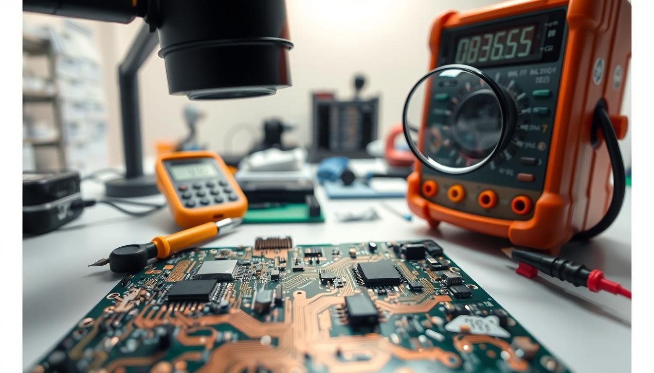
PCBA Reverse Engineering: Capabilities and Considerations
 undergoing reverse engineering. The foreground showcases a partially disassembled PCB, exposing its intricate layers and components. Magnifying tools, schematics, and test equipment surround the board, reflecting the meticulous analysis process. The middle ground features a microscope, probes, and other specialized tools used to study the PCB's circuitry and trace connections. In the background, a complex 3D model of the PCB hovers, highlighting the digital reverse engineering capabilities. The scene is bathed in a warm, focused lighting, conveying the technical expertise and attention to detail required for effective PCBA reverse engineering.")
The secret to extending electronic lifespans lies in a methodical approach to design recovery. We help teams overcome component shortages through precise pcb analysis, identifying modern equivalents using calculations like C = I/ΔV for stable power delivery. This process transforms obsolete boards into upgrade-ready platforms while preserving original functionality.
Advanced pcb imaging techniques reveal hidden design intelligence. X-ray tomography exposes layered connections competitors might conceal, providing actionable insights for product improvement. Our methods go beyond physical inspection—simulated load testing validates component choices before implementation.
Protecting intellectual assets in pcb designs remains paramount. We establish verifiable design records that deter unauthorized replication while enabling legitimate innovation. This dual capability helps companies defend patents and accelerate their own R&D cycles responsibly.
Successful projects balance technical rigor with legal awareness. We prioritize non-destructive analysis where possible, preserving original hardware for future reference. Clear project scoping and phased verification ensure reconstructed pcbs meet current performance standards without compromising historical data integrity.
Applications of PCB Reverse Engineering

How do organizations maintain critical systems when original parts vanish? Strategic reverse engineering solves this challenge through two key applications: sustaining legacy hardware and driving market innovation. These methods keep industrial operations running while revealing opportunities for technological advancement.
End-of-Life Component Replacement
We help teams overcome obsolete part challenges through systematic analysis. When components disappear from markets, we map electrical characteristics and physical dimensions to find modern equivalents. Our process verifies replacements using thermal imaging and load testing before implementation.
Competitive Analysis and Innovation
Understanding competitor designs fuels smarter product development. We decode material choices and manufacturing techniques, revealing cost-saving methods and performance enhancements. This insight helps clients refine their own designs while respecting intellectual property boundaries.
| Application | Key Processes | Outcomes |
|---|---|---|
| Component Replacement | Electrical profiling Mechanical measurement Performance validation |
Extended system lifespan Reduced downtime Cost-effective maintenance |
| Market Analysis | Design pattern mapping Material analysis Cost structure evaluation |
Faster innovation cycles Improved product margins Strategic patent development |
Our approach balances technical precision with practical business needs. For medical equipment manufacturers, we recently restored 1980s imaging systems using modern semiconductors. The updated devices achieved 98% functional parity while reducing power consumption by 40%.
These applications demonstrate how systematic analysis transforms challenges into opportunities. Whether maintaining aging infrastructure or benchmarking industry standards, reconstructed designs provide actionable intelligence for sustainable growth.
Obsolete Component Replacement Strategies
When critical parts disappear from production lines, how do technical teams preserve legacy systems? Our approach combines analytical rigor with practical problem-solving to maintain operational continuity. We focus on two key areas: adapting vintage equipment and applying precise technical methodologies.
Practical Examples: Vintage Equipment
Consider a 1970s audio amplifier requiring transistor replacements. Original parts often have unique gain characteristics (hfe >150) and thermal profiles. Our team recently restored such a system by testing modern semiconductors against performance thresholds derived from circuit analysis.
We calculate critical parameters using Ohm’s Law (V=IR) to verify voltage compatibility. For example, identifying replacements for 2N3055 transistors required matching power dissipation (Pd=115W) and frequency response curves. This ensures functional equivalence without altering original sound quality.
Technical Calculations and Methods
Component identification extends beyond datasheet comparisons. We evaluate thermal resistance (θJA) and saturation voltages (VCE(sat)) through load testing. Signal path verification confirms replacements maintain impedance matching across circuit stages.
Our documentation process captures every modification, creating upgrade blueprints for future maintenance. This method preserves institutional knowledge while enabling sustainable system longevity – crucial for industrial controls and medical devices still operating decades after manufacture.
Intellectual Property Protection and Competitive Analysis
How do leading tech firms shield their breakthroughs from imitation? Intellectual property protection forms the bedrock of sustainable innovation in electronics. We help companies transform reverse engineering into a defensive strategy, using systematic analysis to detect unauthorized use of proprietary designs while respecting legal boundaries.
Our approach combines technical scrutiny with legal safeguards. Through detailed PCB analysis, we identify unique design signatures that prove ownership. This process has helped clients:
| Method | Process | Outcome |
|---|---|---|
| Patent Analysis | Component-level comparison | Infringement detection |
| Material Forensics | Substrate composition testing | Trade secret verification |
| Design Pattern Mapping | Signal path reconstruction | Ownership documentation |
Competitive intelligence requires ethical precision. We analyze rival products to reveal manufacturing efficiencies without compromising proprietary data. Recent work exposed a 23% cost reduction opportunity in power supply designs through material substitutions.
Legal and ethical compliance guides every project. Our teams document findings using court-admissible standards while maintaining strict confidentiality. This dual focus protects clients’ innovations and prevents unintended IP violations during product development.
Effective protection demands collaboration. We bridge engineering insights with legal requirements, helping companies build robust patent portfolios. One client secured three new patents after we identified unique thermal management features in their PCB layouts.
Detailed PCB Reverse Engineering Process
What separates successful design recovery efforts from costly missteps? Our systematic approach transforms physical boards into upgrade-ready blueprints through controlled phases. We combine technical precision with strategic documentation to ensure reliable outcomes.
Step-by-Step Phases Overview
The journey begins with 600dpi scanning and component mapping. Teams use tools like AutoTrace to convert board images into schematic diagrams. Layer-by-layer analysis reveals hidden connections, while material testing identifies substrate properties.
Modern workflows require digital reconstruction of layouts using CAD software. We validate each trace through signal simulation before finalizing designs. This phased method prevents errors that could compromise functional parity.
Challenges and Advanced Techniques
Multilayer boards demand X-ray CT scanning to decode internal pathways without damage. When working with encrypted designs, we employ chemical etching to expose concealed connections—always documenting findings for legal compliance.
For teams seeking deeper insights, our guide to mastering circuit board reverse engineering covers advanced validation methods. These include thermal stress testing and electromagnetic compatibility checks using tools like LTspice.
Every project concludes with rigorous performance benchmarking. We compare original and reconstructed boards under real-world loads, ensuring replacements meet or exceed legacy specifications. This disciplined process turns obsolete systems into platforms for innovation.