In a world where speed defines success, why do 68% of hardware projects still miss critical deadlines? The answer lies in fragmented development processes – a challenge we’ve spent 24 years solving through integrated engineering excellence.
Our team combines wireless innovation with manufacturing precision to transform how smart products reach markets. From industrial scanners to AI-powered robotics, we streamline every technical hurdle – hardware optimization, regulatory compliance, and software integration – into one cohesive workflow.
Ralph Zhao, our VP of MC BU, emphasizes: “True acceleration comes from aligning component-level expertise with system-level vision.” This philosophy drives our approach to solving complex challenges in payment systems, commercial displays, and edge computing applications.
Key Takeaways
- 24-year track record in optimizing connected device development cycles
- Full-spectrum support from prototype validation to mass production
- Pre-certified modules reducing time-to-market by up to 40%
- Cross-industry experience spanning retail, healthcare, and automation
- Dual focus on technical performance and commercial viability
Understanding PCBA Solutions in the IoT Landscape
Behind every smart thermostat or wearable tracker lies an intricate network of components working in harmony. Modern connected systems demand more than just functional parts – they require precision-engineered foundations that balance performance with space constraints.
Definition and Core Components
We approach circuit integration as strategic architecture. Our solutions combine printed circuit boards with microcontrollers, sensors, and wireless modules – all optimized for minimal energy use. Think of it as building a microscopic city where power lines, data highways, and communication towers coexist without interference.
Key elements include:
- Ultra-low-power processors that sip energy like hummingbirds
- Multi-protocol radios supporting Bluetooth, Wi-Fi, and cellular
- Compact sensor arrays capturing environmental data
The Role of PCB Assembly in IoT Devices
Proper assembly transforms individual parts into intelligent systems. Our engineers focus on three critical factors:
- Signal integrity for uninterrupted data flow
- Thermal management in tight spaces
- Manufacturing scalability without quality loss
As one client recently noted: “The difference between functional and exceptional lies in how components converse.” This philosophy drives our work at ESPCBA, where we ensure every millimeter contributes to reliability and speed.
PCBA Solutions for IoT Devices: Enabling Smart Connectivity
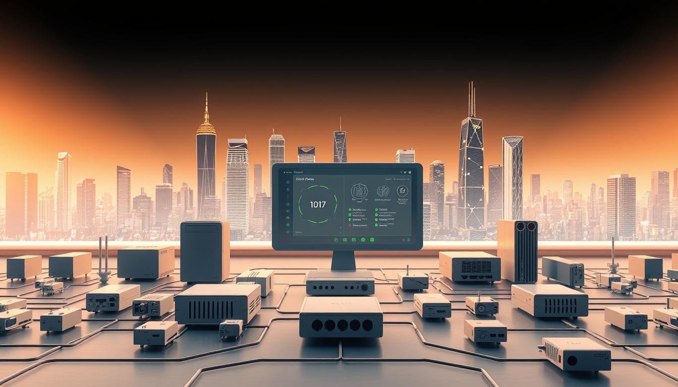
 devices designed by Informic Electronics, showcasing a seamless and intelligent connectivity. In the foreground, a sleek and modern smart home hub surrounded by various IoT sensors and devices, including a smart thermostat, security camera, and smart lighting. The middle ground features a clean, minimalist workspace with a laptop and tablet displaying real-time data and analytics from the connected devices. In the background, a cityscape with skyscrapers and a clear, azure sky, symbolizing the broader network and infrastructure enabling the smart connectivity. The scene is illuminated by warm, diffused lighting, creating a cohesive and visually appealing atmosphere.")
Modern connected systems demand board designs that act as nervous systems – instantly transmitting data while conserving energy. Our approach bridges the gap between component-level innovation and real-world performance.
Customization and Device-Specific Approaches
No two projects share identical requirements. We design circuit assemblies that match exact spatial, power, and functional needs. For wearable health monitors, this means coin-sized boards with week-long battery life. In industrial settings, it translates to ruggedized designs handling extreme temperatures.
Key differentiators include:
- Form factor optimization for space-constrained applications
- Power management systems extending operational lifetimes
- Protocol-specific tuning for interference-free operation
Integration of Sensors and Communication Modules
True intelligence emerges when environmental inputs meet instant data transmission. Our teams combine air quality detectors with 5G modems in pollution monitors. Motion sensors pair with Bluetooth mesh networks in warehouse tracking systems.
One client observed: “The magic happens when humidity readings trigger automated HVAC adjustments within milliseconds.” This seamless interaction drives our multi-protocol integration strategy supporting:
- Simultaneous Wi-Fi/Bluetooth Low Energy operation
- Failover cellular connectivity in remote locations
- Over-the-air update capabilities
Smart home applications showcase this synergy. Thermostats learn occupancy patterns through motion sensors while maintaining constant cloud connections. Energy savings reach 30% without sacrificing user comfort – a balance achieved through meticulous component harmonization.
Advanced Manufacturing Capabilities for IoT Devices

What separates functional prototypes from market-ready products? The answer lies in manufacturing precision that anticipates real-world demands. Our facilities combine cutting-edge technologies with rigorous quality systems to bridge this gap effectively.
High-Density Interconnect and Rigid-Flex Technologies
Modern connected systems demand engineering solutions that shrink component footprints without sacrificing performance. We achieve this through:
- HDI technology with micro/buried vias – 47% space reduction versus conventional designs
- Rigid-flex boards enabling 3D configurations for wearable tech and medical sensors
- Automated impedance control maintaining signal integrity below 0.5dB loss
| Technology | Key Benefit | Typical Application |
|---|---|---|
| HDI Micro Vias | Higher component density | Smartwatches |
| Blind/Buried Vias | Improved signal speed | 5G routers |
| Rigid-Flex PCBs | Enhanced durability | Industrial sensors |
Precision Assembly Processes and Quality Control
Our assembly lines transform complex designs into reliable products through:
- Automated optical inspection (AOI) with 15μm resolution
- X-ray verification for hidden solder joints
- Thermal cycling tests (-40°C to +125°C)
A senior manufacturing engineer notes: “Quality isn’t inspected in – it’s designed through every process interaction.” This philosophy drives our dual-certified facilities (ISO 9001 & IATF 16949) that maintain:
- 99.98% first-pass yield rate
- 24/7 process monitoring systems
- Scalable production from 100 to 1M+ units
Enhancing IoT Device Performance and Reliability
Certifications form the backbone of trustworthy electronics manufacturing. They’re not just framed documents – they’re battle-tested guarantees that every connected system meets exacting operational demands. Our facilities operate under a web of international standards that govern everything from solder joints to environmental impact.
Building Trust Through Compliance
We’ve structured our quality systems around three pillars: precision, repeatability, and accountability. Our ISO 9001:2015 certification ensures every production batch matches strict specifications, while IPC-A-610 adherence guarantees assembly excellence. For medical-grade wearables and automotive trackers, we activate specialized protocols like ISO 13485 and IATF 16949.
Environmental responsibility isn’t an afterthought – it’s engineered into our processes. RoHS and REACH compliance eliminates hazardous substances, aligning with global sustainability goals. UL certification provides third-party validation that our designs won’t fail under stress, crucial for mission-critical applications.
Our testing regimen combines automated checks with real-world simulations. One quality lead explains: “We don’t just verify functionality – we replicate years of use in days.” This approach catches 99.6% of potential issues before products leave our facilities.
Balancing cost and quality requires smart cost-effective manufacturing strategies. Our patented inspection systems maintain rigorous standards across production scales, whether building 500 prototypes or 500,000 units. This scalability stems from 20+ process innovations that reduce waste while boosting reliability.
Performance optimization starts at the design phase. We employ failure mode analysis to preemptively address thermal stress and signal degradation. The result? Connected systems that deliver consistent operation through temperature swings, moisture exposure, and constant data transmission.
Streamlined Production and Global Support for IoT Solutions
When product timelines shrink faster than component sizes, smart manufacturing becomes the ultimate competitive edge. We transform complex builds into seamless workflows through precision-engineered services that adapt to evolving market demands.
Turnkey Assembly and Rapid Prototyping Services
Our complete production package handles everything from raw materials to shipment-ready units. Clients save 18% in operational costs through:
| Service | Time Savings | Key Benefit |
|---|---|---|
| One-Click Prototyping | 72-hour turnaround | Instant design validation |
| Box Build Assembly | 40% faster scaling | End-to-end integration |
| Conformal Coating | 3X lifespan increase | Environmental protection |
Rapid iteration cycles powered by automated BOM analysis cut development phases by 65%. A project lead recently noted: “What used to take three revisions now happens in one seamless build.”
Comprehensive Support and Global Logistics
We maintain 97% on-time delivery rates through integrated supply chain management. Our global network ensures:
- Real-time production tracking across 12 time zones
- Customs-cleared shipping to 150+ countries
- Regional testing hubs for localized compliance
Post-deployment support includes firmware updates and failure analysis. As one partner observed: “Their team becomes an extension of our engineering department – proactive, knowledgeable, and available.”
From prototype validation to million-unit runs, we bridge the gap between innovative concepts and market-ready products. Our data-driven approach eliminates guesswork, delivering IoT applications that perform as designed – everywhere.
Conclusion
The future of connected technology demands more than components – it requires holistic integration of design expertise and manufacturing precision. We bridge this gap through two decades of refining processes that balance innovation with practical application demands.
Our approach transforms complex technical requirements into reliable products. From smart home ecosystems to industrial monitoring systems, we ensure every circuit assembly meets rigorous performance benchmarks. Strategic PCB design remains central to achieving energy efficiency and data integrity in modern applications.
Trusted partnerships drive progress. As industry leaders, we prioritize scalable production methods that adapt to evolving connectivity standards. Recent advancements in multi-layer board architectures demonstrate how intelligent layouts enhance device lifespans while maintaining compact form factors.
True innovation emerges when technical capability meets real-world user needs. Whether optimizing thermal management or streamlining high-density assembly processes, our teams deliver solutions built for tomorrow’s challenges. Let’s engineer smarter systems – together.