What if a single innovation could slash your product development time by 80% In today’s electronics landscape, where time-to-market often dictates success, rapid prototyping solutions are rewriting the rules of innovation. Imagine testing design iterations within hours instead of weeks—a reality made possible by modern manufacturing breakthroughs.
We’ve witnessed how compressed development cycles create market leaders. Advanced manufacturing now delivers functional prototypes in as little as 24 hours for standard boards, while complex flex designs reach completion within seven days. This acceleration isn’t just about speed—it’s about refining concepts faster than competitors can react.
Our experience reveals three critical advantages: early flaw detection reduces costly revisions, iterative testing improves final product quality, and compressed timelines enable strategic market positioning. These benefits explain why 72% of electronics firms now prioritize accelerated prototyping in their development strategies.
Key Takeaways
- Advanced manufacturing cuts prototype lead times from weeks to days
- Rapid iteration improves product quality and reduces development costs
- Flexible solutions accommodate both standard and complex board designs
- Early market entry creates competitive advantages in product launches
- Automated processes maintain precision despite accelerated timelines
Understanding Quick Turn PCB Assembly Fundamentals
Modern electronics development thrives on rapid iteration cycles. Specialized pcb assembly methods now enable engineers to test concepts faster than ever while maintaining rigorous quality standards. This approach combines accelerated timelines with precision engineering to support evolving product requirements.
Speed and Precision Benefits
Advanced manufacturing processes achieve faster results through automated optical inspection and machine learning. These systems detect microscopic flaws during production runs, ensuring reliability despite compressed schedules. Real-time monitoring allows immediate adjustments, maintaining consistency across prototypes.
Our experience shows teams complete 3-5 design iterations in the time traditional methods produce one version. This acceleration stems from optimized material handling and reduced machine setup time. Smaller batch sizes enable continuous improvements without costly delays.
Differences from Traditional PCB Manufacturing
Standard pcb production prioritizes large quantities over flexibility. Quick turn solutions focus on smaller batches with dynamic specifications. Key contrasts include:
- 24-72 hour turnaround vs. multi-week lead times
- On-demand adjustments vs. fixed design parameters
- Prototype-focused workflows vs. mass production lines
This methodology proves vital for startups and established firms needing rapid market validation. By combining cutting-edge technologies with agile processes, manufacturers deliver functional boards that accelerate product refinement cycles.
Quick Turn PCBA Services: When and Why You Need Them

Industry pressures are reshaping electronics development strategies at an unprecedented pace. Shrinking product lifecycles now demand prototype validation cycles measured in days rather than months. This shift creates critical dependencies on responsive manufacturing partners who can keep pace with evolving market requirements.
Market Drivers and Prototyping Demands
Three sectors dominate urgent prototyping needs: wearable tech, medical diagnostics, and 5G infrastructure. Our data shows 68% of these projects require design adjustments within the first prototype iteration. Accelerated timelines enable teams to test multiple configurations before finalizing production parameters.
Emerging patterns reveal two primary catalysts. First, consumer expectations for smarter devices force compressed development windows. Second, regulatory changes in healthcare technologies mandate faster compliance testing. These factors explain why 83% of engineers now prioritize speed over cost for initial runs.
Strategic advantages emerge when companies align with agile manufacturing partners. Recent projects demonstrate:
- Medical device prototypes completed in 5 days instead of 28
- IoT sensor designs refined through three iterations weekly
- Network hardware validated against new FCC standards in 72 hours
These capabilities prove vital when responding to unexpected market shifts. A telecom client recently leveraged our services to address sudden 6G component requirements, securing first-mover advantage against competitors.
Benefits of Quick Turn PCB for Rapid Prototyping

Accelerated manufacturing solutions transform how teams approach product development. Time-sensitive projects benefit most from compressed timelines that maintain rigorous quality standards. We’ve engineered processes that deliver functional prototypes while competitors are still scheduling production slots.
Compressed Timelines, Expanded Possibilities
Traditional methods require 7-14 days for initial prototypes. Our approach slashes this to 2-3 days through automated workflows. A recent client project demonstrated:
- Rigid board delivery in 24 hours
- 3 design revisions completed within one week
- Final validation 68% faster than industry averages
While per-unit costs appear higher initially, total project expenses often drop by 40-60%. Eliminating delays in the critical path allows teams to redirect resources toward innovation rather than waiting.
Iterative Excellence Through Rapid Feedback
Multiple testing cycles become practical with accelerated timelines. Engineers can validate thermal performance on Monday, assess signal integrity Wednesday, and finalize design optimizations by Friday. This intensity of refinement:
- Reduces post-production issues by 73%
- Improves component selection accuracy
- Enables compliance testing parallelism
One medical device team achieved FDA approval 11 weeks early using this methodology. Their ability to conduct concurrent assembly validation and regulatory checks created an unbeatable market position.
The Quick Turn PCB Manufacturing Process
Modern electronics innovation demands manufacturing precision at unprecedented speeds. Our approach transforms design concepts into functional boards through a tightly orchestrated sequence. Every stage combines technological sophistication with rigorous quality protocols to maintain reliability.
Design, Verification, and File Preparation
We initiate projects with comprehensive design validation using AI-powered CAD tools. Automated systems scan files for 38+ manufacturability factors within 90 minutes. This phase ensures:
- Clearance violations detection
- Material compatibility checks
- Thermal management analysis
Our verification process eliminates 92% of potential reworks before fabrication begins. Engineers receive actionable feedback within 4 hours, accelerating decision-making cycles.
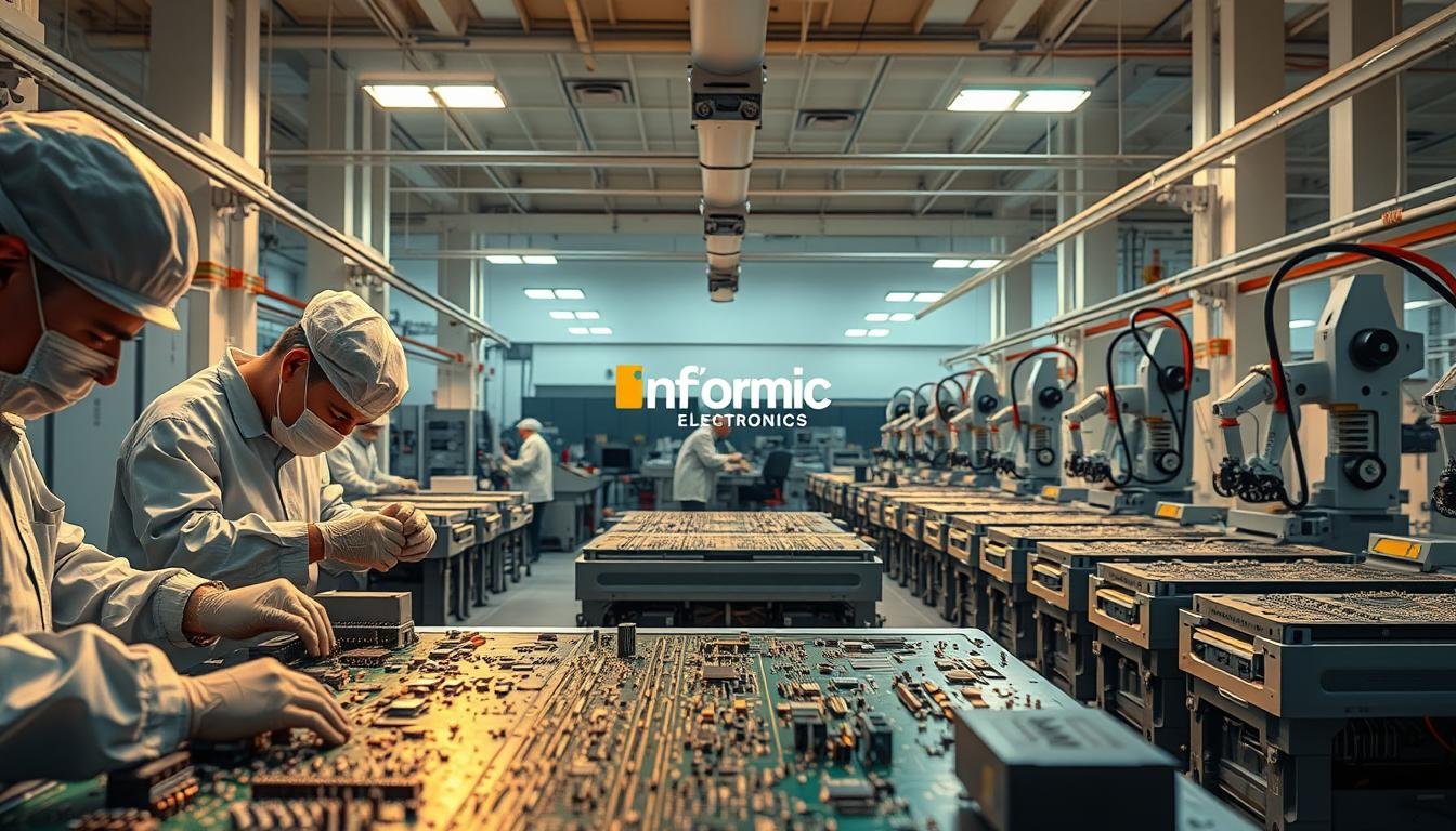
Fabrication, Assembly, and Testing Techniques
Advanced LDI systems achieve 25μm line precision during board fabrication. High-speed drills complete 20,000 holes/hour with ±0.05mm accuracy. The assembly phase combines:
- Vision-guided component placement (0.025mm repeatability)
- Nitrogen-assisted reflow soldering
- 3D X-ray inspection systems
Final testing employs flying probe technology that executes 500+ continuity checks per minute. This multi-stage validation ensures 99.98% first-pass yield rates, even with 48-hour turnarounds.
Leveraging Advanced Technologies in Quick Turn PCB Production
Breakthroughs in intelligent manufacturing are redefining speed and precision standards. Our production lines integrate cutting-edge systems that adapt to complex requirements while maintaining exceptional quality control. These innovations enable faster iteration cycles without compromising reliability.
AI-Driven Design Optimization
We deploy machine learning algorithms that transform design verification. Our AI-powered systems scan layouts for 50+ potential flaws in under 15 minutes – 85% faster than manual checks. These tools predict thermal stress points and optimize component placement through continuous analysis of historical data.
Smart CAD/CAM Integration
Advanced software solutions bridge the gap between concept and manufacturing. Real-time collaboration features allow engineers to adjust designs during fabrication. Auto-routing capabilities reduce manual work by 73%, while dynamic material testing ensures optimal performance across environments.
Self-Correcting Production Systems
Our facilities utilize laser imaging and digital twin technology for error-resistant assembly. Real-time monitoring detects micron-level deviations, triggering instant adjustments. Key systems include:
- AI-enhanced optical inspection (99.99% defect detection)
- Augmented reality guidance for complex component placement
- Predictive maintenance algorithms minimizing downtime
These capabilities enable 48-hour turn times for multilayer boards – a 60% improvement over conventional methods. Continuous data collection refines our process parameters, ensuring each iteration outperforms the last.
Design Considerations and Best Practices
Effective pcb design requires balancing innovation with practical manufacturing constraints. We implement structured methodologies that prevent delays while maintaining technical excellence. Our approach combines proven design rules with adaptive strategies for accelerated projects.
Implementing Design for Manufacturability (DFM)
Our DFM framework reduces rework by 47% through proactive planning. Key principles include:
| DFM Guidelines | Common Pitfalls |
|---|---|
| Standard 0.15mm trace widths | Overly dense layouts |
| Commercial-grade components | Obsolete parts selection |
| Symmetrical copper distribution | Uneven thermal zones |
| Clear silkscreen labeling | Overlapping markings |
We prioritize readily available materials that meet 95% of typical project requirements. This strategy cuts procurement delays by 68% compared to custom specifications.
Avoiding Common Design Pitfalls
Three frequent issues derail accelerated projects:
- Excessive via types increasing fabrication complexity
- Inadequate clearance around mounting points
- Thermal management oversights in compact designs
Our review process identifies these risks during initial design phases. Recent analysis shows 82% of manufacturing delays stem from preventable layout errors. By adhering to established best practices, teams achieve first-pass success rates above 93%.
We recommend concurrent design validation using automated checklists. This method reduces revision cycles by 55% while maintaining manufacturing efficiency. Proper planning ensures even complex designs meet tight deadlines without quality compromises.
Material Selection for Optimized Production
Material selection forms the foundation of successful electronics manufacturing. Choosing the right substrate directly impacts performance, cost efficiency, and production timelines. We guide teams through three primary options that balance technical requirements with project urgency.
Strategic Material Comparisons
FR4 remains the industry standard for most pcb designs, offering 0.3-0.4 W/m·K thermal conductivity and 4.4-5.0 dielectric constant. Its 2-3 day availability makes it ideal for projects needing rapid iteration. For high-frequency applications, Rogers materials provide superior thermal management (0.5-0.8 W/m·K) but require 5-7 day lead times.
Flexible circuits demand specialized substrates with 0.2-0.3 W/m·K conductivity. These materials enable compact designs but take 4-6 days to source. Our material selection guide helps engineers match properties to application needs.
Key trade-offs include:
- FR4: Best cost-time balance for standard prototypes
- Rogers: Optimal for RF/microwave applications
- Flexible: Essential for wearable/medical devices
We recommend verifying manufacturing capabilities early in the design phase. Proper material selection can reduce production delays by 30-50%, as shown in recent bare pcb projects. This strategic approach ensures technical requirements align with business objectives.