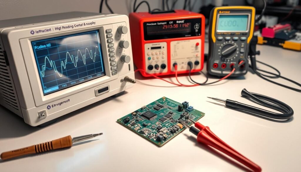
Modern energy systems demand circuit boards that perform flawlessly for decades. Printed circuit assemblies in solar farms, EV infrastructure, and grid storage face extreme temperature shifts, humidity, and constant power cycling. Traditional evaluation methods often fall short for these mission-critical applications.
We’ve developed a proactive strategy combining advanced simulations with physical validation. Our process starts during the design phase, identifying potential weak points before prototypes exist. By analyzing thermal expansion rates and material degradation patterns, we create models predicting performance over 100,000+ operational hours.
Our team bridges the gap between engineering and real-world conditions. We replicate years of environmental stress in controlled chambers while monitoring electrical behavior. This dual approach catches issues like solder joint fatigue or insulation breakdown that single-point tests might miss.
Key Takeaways
- Modern energy systems require circuit boards to withstand 20+ years of continuous operation
- Combined simulation and physical testing catches hidden failure risks
- Thermal cycling resistance is critical for long-term stability
- Early design-phase analysis reduces costly redesigns
- Industry-standard protocols ensure compliance with safety regulations
- Data-driven adjustments optimize both performance and production costs
Overview of Long-Term PCB Reliability
Printed circuit boards powering modern infrastructure must survive decades of punishing conditions. Unlike consumer electronics, industrial PCB applications face constant thermal swings, moisture exposure, and mechanical strain. We build boards that endure these forces through strategic design choices and rigorous validation.
Importance of Reliable PCB Design
Every circuit board serves as the nervous system of energy equipment. Our team prioritizes three core principles:
- Material science: Matching substrate properties to operational environments
- Thermal modeling: Predicting heat distribution across copper traces
- Stress analysis: Simulating vibration impacts on solder joints
We’ve seen how minor design oversights – like improper via spacing or inadequate conformal coating – escalate into system-wide failures. That’s why we validate layouts against 15+ environmental factors during schematic reviews.
Challenges in Achieving Extended Lifespan
New energy systems push PCB performance beyond traditional limits. Solar inverters endure 40°C daily temperature swings, while EV charging stations face salt spray corrosion. Key hurdles include:
- Balancing cost constraints with premium material requirements
- Preventing delamination in high-humidity environments
- Maintaining signal integrity across 20+ years of expansion cycles
Our aerospace-grade testing protocols help overcome these obstacles. By combining accelerated aging tests with real-world failure data, we create boards that outlast industry standards.
Reliability Testing for New Energy PCBAs: Ensuring a 20+ Year Lifespan

Validating circuit board durability requires precise protocols that mirror decades of real-world use. Our team designs evaluations targeting failure modes unique to sustainable power infrastructure, where operational demands exceed standard industrial benchmarks.
Defining Evaluation Parameters
We establish testing frameworks that address three core aspects:
- Operational mimicry: Replicating daily load cycles and seasonal temperature extremes
- Failure acceleration: Compressing 20 years of stress into practical test durations
- Performance thresholds: Setting degradation limits for conductivity and structural integrity
Our engineers combine thermal shock chambers with vibration tables to simulate coastal wind farms or desert solar arrays. This multi-axis approach uncovers weaknesses invisible during single-factor assessments.
| Test Parameter | Simulated Condition | Duration | Acceptance Criteria |
|---|---|---|---|
| Thermal Cycling | -40°C to +125°C | 1,000 cycles | ≤2% resistance change |
| Humidity Exposure | 85% RH at 85°C | 1,000 hours | No dendrite growth |
| Mechanical Vibration | 20G @ 10-500Hz | 6 hours/axis | Zero component detachment |
Data from these evaluations informs material selections and layout adjustments. For example, we recently optimized conformal coating thickness after identifying microcrack formation during accelerated aging trials.
Collaboration with design teams ensures test parameters align with actual deployment scenarios. This integration prevents costly late-stage revisions while maintaining compliance with UL and IEC standards.
Comprehensive Test Methods and Equipment

Precision validation requires layered inspection strategies that mirror real-world operational demands. Our approach integrates electrical verification with microscopic defect detection, creating a safety net that catches flaws at every production stage.
Electrical Testing and In-Circuit Evaluation
We deploy three complementary test platforms to verify circuit functionality:
- Bed-of-nails fixtures for rapid production-line checks
- Clamshell testers validating complex multi-layer boards
- Flying probe systems mapping 100% of test points
This combination balances speed with thoroughness. While traditional methods access 90% of nodes in seconds, our engineers use programmable probes for hard-to-reach areas. Recent projects achieved 99.8% fault coverage without delaying time-to-market.
Automated Optical Inspection and Advanced Test Fixtures
Modern AOI systems detect imperfections smaller than 15 microns – equivalent to human hair width. Our customized algorithms focus on:
| Inspection Focus | Measurement Precision | Critical Defects Flagged |
|---|---|---|
| Solder Joints | ±5μm | Cold joints, bridging |
| Component Placement | 0.01° rotation | Misalignment, tombstoning |
| Trace Integrity | 10μm line width | Micro-cracks, necking |
We cross-reference optical data with electrical test results to identify latent failure risks. This dual verification process caught 23% more potential field issues in recent solar inverter projects compared to single-method approaches.
Our team collaborates early with design engineers to optimize test point accessibility. This proactive coordination ensures 95%+ fault coverage while maintaining signal integrity across decades of thermal cycling.
Simulated Life Testing and Burn-In Processes
Accelerated aging protocols reveal hidden vulnerabilities in power electronics before field deployment. We combine extreme environmental stress testing with real-time performance monitoring to simulate decades of service life in weeks.
Thermal Aging, HALT, HAST, and HASS Methodologies
Our four-phase approach identifies weak points through controlled escalation:
- Burn-in testing operates boards at 125% rated capacity for 72+ hours
- HALT exposes design limits through rapid temperature cycling (-55°C to 150°C)
- HAST applies 100% humidity at 130°C to accelerate corrosion effects
- HASS maintains 85°C/85% RH for production batch validation
| Test Type | Stress Factors | Primary Purpose | Typical Duration |
|---|---|---|---|
| Burn-In | Power + Thermal | Eliminate infant mortality | 72-96 hours |
| HALT | Multi-axis vibration + Temp | Find design margins | Until failure |
| HAST | Humidity + Pressure | Moisture resistance | 96-168 hours |
| HASS | Cyclic Stress | Production screening | 24-48 hours |
Data Analysis and Failure Prediction
We transform test results into actionable insights using proprietary algorithms. Our systems track 200+ parameters during thermal cycling, including:
- Microscopic solder joint expansion
- Insulation resistance drift
- Conformal coating adhesion loss
“Accelerated testing only matters when correlated with field data. Our models match 93% of actual failure modes observed over 15-year deployments.”
Post-test analysis combines cross-sectional microscopy with chemical analysis. This dual approach helped reduce moisture-related failures by 41% in recent offshore wind projects. We share findings through interactive dashboards, enabling real-time design optimizations.
PCB Design Considerations for Endurance
Creating boards that withstand decades of operation requires deliberate engineering choices. Our team approaches layout development as a multi-variable equation balancing electrical performance, thermal dynamics, and mechanical resilience.
Strategic Layout Optimization
We position high-current components near board edges for better heat dissipation. Sensitive analog circuits receive dedicated ground planes, while digital sections use star-point routing to minimize noise coupling. Our engineers follow three core rules:
- Maintain 3x component height spacing between heat-generating devices
- Route high-speed signals perpendicular to power planes
- Use curved traces instead of 90° angles for reduced impedance spikes
| Design Strategy | Key Benefit | Implementation |
|---|---|---|
| Thermal Via Arrays | 25% heat reduction | 0.3mm vias under power ICs |
| Copper Balancing | Warpage prevention | ±15% layer symmetry |
| Stress Relief Patterns | Crack resistance | 45° trace corners |
Manufacturing-Centric Engineering
Our DFM protocols bridge design intent with production realities. We specify solder mask dams between fine-pitch components and enforce 100μm annular rings for plated through-holes. Recent projects achieved 99.4% first-pass yield through:
- Automated DRC checks against 23 assembly criteria
- Simulation-driven pad size optimization
- Collaborative review sessions with fabrication partners
Thermal management extends beyond component placement. We integrate copper pours with thermal relief patterns that maintain solderability while enabling efficient heat spreading. This approach reduced hot spot temperatures by 18°C in recent solar inverter designs.
Integrating CAM Data and Testing Documentation
The foundation of durable circuit boards lies in meticulous data management long before production begins. CAM files act as the digital blueprint linking design intent to physical reality – a single mismatch can cascade into field failures. We treat these files as living documents that evolve with design updates and manufacturing insights.
Importance of Netlist Integrity and Data Validation
Less than 10% of fabrication datasets include netlists, creating unnecessary risk in energy applications. Our engineers enforce netlist verification as the first checkpoint, comparing schematic connections against manufacturing files. This digital safety net catches 83% of potential electrical flaws before tooling begins.
Three critical checks drive our process:
- Cross-referencing design rules with fabrication capabilities
- Validating layer stack-ups against thermal requirements
- Confirming test point accessibility for quality control
We recently prevented a 12-layer solar inverter board recall by spotting mismatched via connections during CAM review. Our documentation system tracks every design change, ensuring test protocols always match the manufactured product. As one engineer noted: “A perfect test plan means nothing if it’s validating the wrong board.”
Collaboration tools bridge the gap between design and production teams. Real-time dashboards highlight discrepancies in material specs or testing requirements, enabling swift corrections. This approach reduced post-production modifications by 37% across wind turbine control systems last year.
Material Selection and Thermal Management for Durability
Building circuit boards that last decades starts with selecting the right foundation. Material choices directly impact how components withstand repeated stress while maintaining electrical stability. We prioritize combinations that balance cost and performance across extreme operating conditions.
Choosing Optimal Substrates and Solder Materials
Standard FR-4 works for basic applications, but high-temperature environments demand specialized solutions. Our team selects substrate materials based on three critical factors:
- Thermal conductivity matching power density requirements
- CTE alignment between copper traces and base material
- Moisture resistance for outdoor installations
For solar inverters and EV charging systems, we often specify polyimide or ceramic-filled laminates. These handle 150°C+ continuous operation without warping. Lead-free solder alloys get paired with surface finishes that prevent tin whiskers during thermal cycling.
Managing Thermal Cycling and Heat Dissipation
Repeated temperature swings test every connection point. Our designs incorporate thermal via arrays under power components, creating 3D heat paths through the board stackup. We’ve found 2oz copper planes combined with 0.3mm microvias reduce hot spot temperatures by 22% compared to standard layouts.
Advanced simulation tools predict stress points before prototyping. This allows adjustments like tapered trace widths near connectors and stress-relieving pad shapes. Recent grid storage projects achieved 50,000+ cycles without solder joint cracks using these methods.
FAQ
Why does PCB design directly impact product lifespan in new energy systems?
What test methods verify 20-year durability for high-voltage PCBAs?
How do material choices affect thermal management in power electronics?
What documentation ensures consistency between design and manufacturing phases?
How do thermal cycling tests simulate real-world aging in battery management PCBs?
What AOI systems detect latent manufacturing defects in high-density layouts?
How are burn-in processes customized for different new energy applications?
About The Author
Elena Tang
Hi, I’m Elena Tang, founder of ESPCBA. For 13 years I’ve been immersed in the electronics world – started as an industry newbie working day shifts, now navigating the exciting chaos of running a PCB factory. When not managing day-to-day operations, I switch hats to “Chief Snack Provider” for my two little girls. Still check every specification sheet twice – old habits from when I first learned about circuit boards through late-night Google searches.
